TED interview with Elon Musk has a couple of interesting notes about Tesla autonomous car plans:
"Tesla Model 3 is coming in July, Musk says, and it’ll have a special feature: autopilot. Using only passive optical cameras and GPS, no LIDAR, the Model 3 will be capable of autonomous driving. “Once you solve cameras for vision, autonomy is solved; if you don’t solve vision, it’s not solved … You can absolutely be superhuman with just cameras.”
Musk says that Tesla is on track for completing a fully autonomous, cross-country LA to New York trip by the end of 2017. “November or December of this year, we should be able to go from a parking lot in California to a parking lot in New York, no controls touched at any point during the entire journey,” Musk says."
Sunday, April 30, 2017
Friday, April 28, 2017
Lund University Camera Reaches 20 Tera-fps Speed
Lund University, Sweden, announces that its researches were able to achieve 200fs temporally resolving camera. Their paper has been accepted for publication in "Light: Science & Applications" journal and available on-line: "FRAME: femtosecond videography for atomic and molecular dynamics" by Andreas Ehn, Joakim Bood, Zheming Li, Edouard Berrocal, Marcus Aldén, and Elias Kristensson:
"In this Letter, we present a laser probe-based method that unifies the aforementioned aspects and is capable of producing a video sequence of non-repetitive dynamic events at femtosecond timescales and beyond for spectroscopy. Our method, called Frequency Recognition Algorithm for Multiple Exposures (FRAME), allows acquisition of a series of laser-induced images at frame rates that are limited only by the laser pulse duration. Here, we used femtosecond laser pulses to demonstrate videography with record high sub-ps (THz) temporal resolution, although attosecond laser pulses could, in principle, increase the frame rate into the PHz regime. The novelty of the FRAME concept lies in superimposing a structural code onto the illumination to encrypt a single event that is then deciphered in the data post-processing. Because each image in the video sequence is extracted by using a unique spatial code, the method does not rely on a specific optical wavelength or laser bandwidth, and hence can be used for spectroscopic measurements. Here, we provide a proof-of-principle demonstration of our method by performing imaging light-in-flight – often regarded as the gold standard experiment for ultrafast imaging at 5 THz, a timescale on which even light appears stationary on a macroscopic scale."

Although the paper talks about 200fs temporal resolution, the University demo shows 50fs time step between the frames of their video:
Conversant NPE Buys 29 CIS Patents from Dongbu
IAM-Media: Ottawa, Canada-based Conversant NPE has acquired 29 image sensor patents from Dongbu HiTek, USPTO assignments records reveal.
Dongbu’s somewhat unusual willingness to sell its IP seems to be related to previous debt problems and the financial woes of its parent, the Dongbu Group chaebol (conglomerate). In the previous years, IAM-Media identified Dongbu HiTek as one of the top 15 sellers of patents worldwide:

Dongbu’s somewhat unusual willingness to sell its IP seems to be related to previous debt problems and the financial woes of its parent, the Dongbu Group chaebol (conglomerate). In the previous years, IAM-Media identified Dongbu HiTek as one of the top 15 sellers of patents worldwide:

Samsung to Add One More CIS Fab
PulseNews: Samsung is to convert Line 11 in Hwaseong fab in Gyeonggi Province active since mid-2000s to CIS production starting the first half next year to meet growing demand for mobile imaging, high-end photography, and security and surveillance applications. Sony is said to have a solid lead on the CIS narket, controlling 44.5% of global supply including iPhones. Samsung is at second place with a share of 15% as it supplies the imagers for Samsung premium phones.
SeekingAlpha quotes Samsung representative on that: "we’re planning to convert Line 11 to CIS given the fact that strong image sensor demand...
And to give thorough detail about the CMOS image sensor CIS that we’ll be using part of Line 11 to produce as you know with the increased adoption of dual camera, the application has itself been growing and also in addition to these mobile cameras we’re also trying to expand the applications to VR automotive as well as 360 degree cameras. So to respond to market demand as well as customer request, we will be converting part of Line 11 for our CIS production. Our target is to start mass production first half of 2018 but that is subject to market demand as well as customer request."
 |
| Samsung Hwaseong plant |
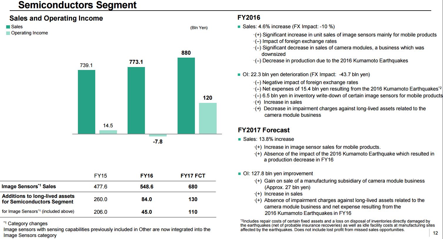
Sony Reports FY2016 Results
Sony reports its quarterly and yearly results. Few slides showing image sensor business status and the new year forecas:


From the Sony PR:
Results for a fiscal year ended on March 31, 2017:
"Sales increased 4.6% year-on-year (a 15% increase on a constant currency basis) to 773.1 billion yen (6,903 million U.S. dollars). This increase in sales was primarily due to a significant increase in unit sales of image sensors mainly for mobile products, partially offset by the impact of foreign exchange rates, a significant decrease in sales of camera modules, a business which was downsized, and the decrease in production due to the 2016 Kumamoto Earthquakes. Sales to external customers increased 10.1% year-on-year.
Operating loss of 7.8 billion yen (70 million U.S. dollars) was recorded, compared to operating income of 14.5 billion yen in the previous fiscal year. This significant deterioration in operating results was primarily due to the negative impact of foreign exchange rates, the above-mentioned expenses resulting from the 2016 Kumamoto Earthquakes, and a 6.5 billion yen (58 million U.S. dollars) write-down of inventories of certain image sensors mainly for mobile products. This deterioration was partially offset by the above-mentioned year-on-year increase in sales and the decrease in impairment charges against long-lived assets related to the camera module business.
During the current fiscal year, there was a 43.7 billion yen negative impact from foreign exchange rate fluctuations."
Last quarter results:
"In the Semiconductors segment, sales increased significantly due to an increase in unit sales of image sensors. Sales to external customers also increased significantly year-on-year."
Reuters comments: "Image sensors have emerged as the biggest contributor to profit growth, as operations at a factory damaged by earthquakes a year ago return to normal just as smartphone makers are increasingly adopting dual-lens rear cameras in their handsets, requiring extra sensors.
"The market is growing for higher-end models with dual-lens rear cameras or with high-performance front cameras designed for self-shooting," Chief Financial Officer Kenichiro Yoshida said at an earnings briefing. "That serves as a tailwind for us."
Sony forecast its chip division, which includes image sensors, to return to profit this year, at 120 billion yen.
To meet increased demand, it will more than double capital expenditure on image sensors to 110 billion yen, raising production capacity by 13.6 percent by the end of March."
Hynix to Separate 8-inch Foundry Business
ETNews: SK Hynix is separating its 8-inch Foundry Business Department as an independent subsidiary tentatively named "SK Hynix System IC". The 8-inch M8 fab has a capacity of 100K wafers per year and image sensors is one of its main specialties.
According to IHS, SK Hynix’s Foundry Business made about $140M in sales last year, less that 1% of the whole company sales of $15.2b. The foundry business registered a loss last year.
SK Hynix will continue production of high-megapixel image sensor products of over 13MP at its 12-inch M10 fab.
According to IHS, SK Hynix’s Foundry Business made about $140M in sales last year, less that 1% of the whole company sales of $15.2b. The foundry business registered a loss last year.
SK Hynix will continue production of high-megapixel image sensor products of over 13MP at its 12-inch M10 fab.
Thursday, April 27, 2017
Dynamic Photodiodes are Said to Save Power in Heartrate Sensors
PRNewswire: Switzerland-based ActLight presents its Heartrate Sensor for wearables, said to reduce power consumption by 80% compared to what is currently available on the market, while delivering the same performance. The Heartrate sensor is based on ActLight's proprietary Dynamic Photo Diode (DPD) technology and has been developed in co-operation with a global MedTech semiconductor vendor and EPFL.
In smartwatches and wearables, up to 80% of the power consumption is said to be related to heartrate monitoring when it is activated. Already tested and calibrated, ActLight's heartrate sensor is ready to be produced in large series to equip next generation wearables with reduced power consumption.
"Increased interest in fitness and wellness - has necessitated more affordable, precise, wearable sensing options. Our technology offers unique competitive advantages to our partners when compared to existing Photo Diodes used in wearable heartrate solutions," stated Serguei Okhonin, CEO of ActLight. "ActLight is now working with a number of partners to bring this technology into consumer electronics and MedTech grade solutions. We are open for IP licensing of our patented DPD technology that we own 100%," Okhonin continued.
EPFL publishes an article and an Youtube video on the new product:
Wednesday, April 26, 2017
ARM Announces 24b HDR Imaging and Vision Co-Processor
Anandtech: ARM announces Mali-C71 ultra-wide dynamic range (UWDR) ISP with up to 24 stops DR for automotive camera applications. It removes noise and processes the multiple exposures from the camera, creates an ultra-WDR frame and sends it across to a display or a computer vision engine. The Mali-C71 is the first imaging product since ARM acquired Apical in 2016. OmniVision Technologies, a leading developer of advanced digital imaging solutions, has welcomed the development:
“OmniVision has been closely collaborating with the ARM ISP team (formerly Apical) for several years now, and see the Mali-C71 as an important advancement in image signal processing for emerging automotive applications. ARM’s expertise in ISP technology together with OmniVision’s best-in-class HDR image sensor technologies offers an industry leading solution for our automotive customers,” said Will Foote, senior partnership manager, OmniVision.
The Mali-C71 brings advanced error detection with more than 300 dedicated fault detection circuits to enable system-level certification to the modern automotive standards (ISO26262, ASIL D and IEC 61508, SIL3). It is able to process up to 4 real-time cameras and 16 camera streams with a single pipeline:
 |
| Mali-C71 block diagram |


Cadence Vision DSP Certified as Khronos OpenVX 1.1 Conformant
Cadence Tensilica Vision P-Series DSPs are said to be the first imaging/vision DSPs to pass Khronos Group’s conformance tests for the OpenVX 1.1 spec. This enables faster development of computer vision and imaging applications on Tensilica Vision P-Series DSPs being deployed in applications processors for mobile, automotive, drone, security, AR/VR and other markets. Applications developed using the standard OpenVX 1.1 API can be compiled and run on Tensilica Vision DSPs without any code changes.
Tuesday, April 25, 2017
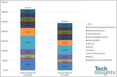
Cameras are 9.25% of Samsung Galaxy S8 Cost
TechInsights completes its teardown report of Samsung Galaxy S8, and publishes an estimation of the phone's BOM. The cameras are about 9.25% of the BOM, down from 10% in the last year's S7:


Monday, April 24, 2017
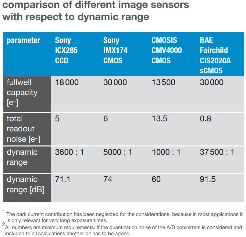
PCO Compares Image Sensors DR
PCO DR whitepaper compiles a table comparing various image sensors DR. The rolling shutter BAE sCMOS sensor outperforms all global shutter alternatives on DR:

Sunday, April 23, 2017
Image Sensor Reliability, Variations, and Drifts over Time
Albert Theuwissen has a unique experience with image sensor statistics and their parameters changing over time when his students run through the same devices characterization, course after course, year after year. So, he came up with a brilliant idea to present his knowledge in a report on CMOS sensors reproducibility, variability, and reliability. The first info about the report is expected to be available in a few weeks.
Saturday, April 22, 2017
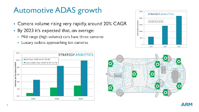
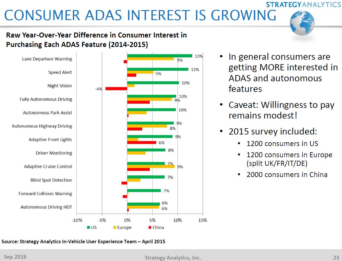
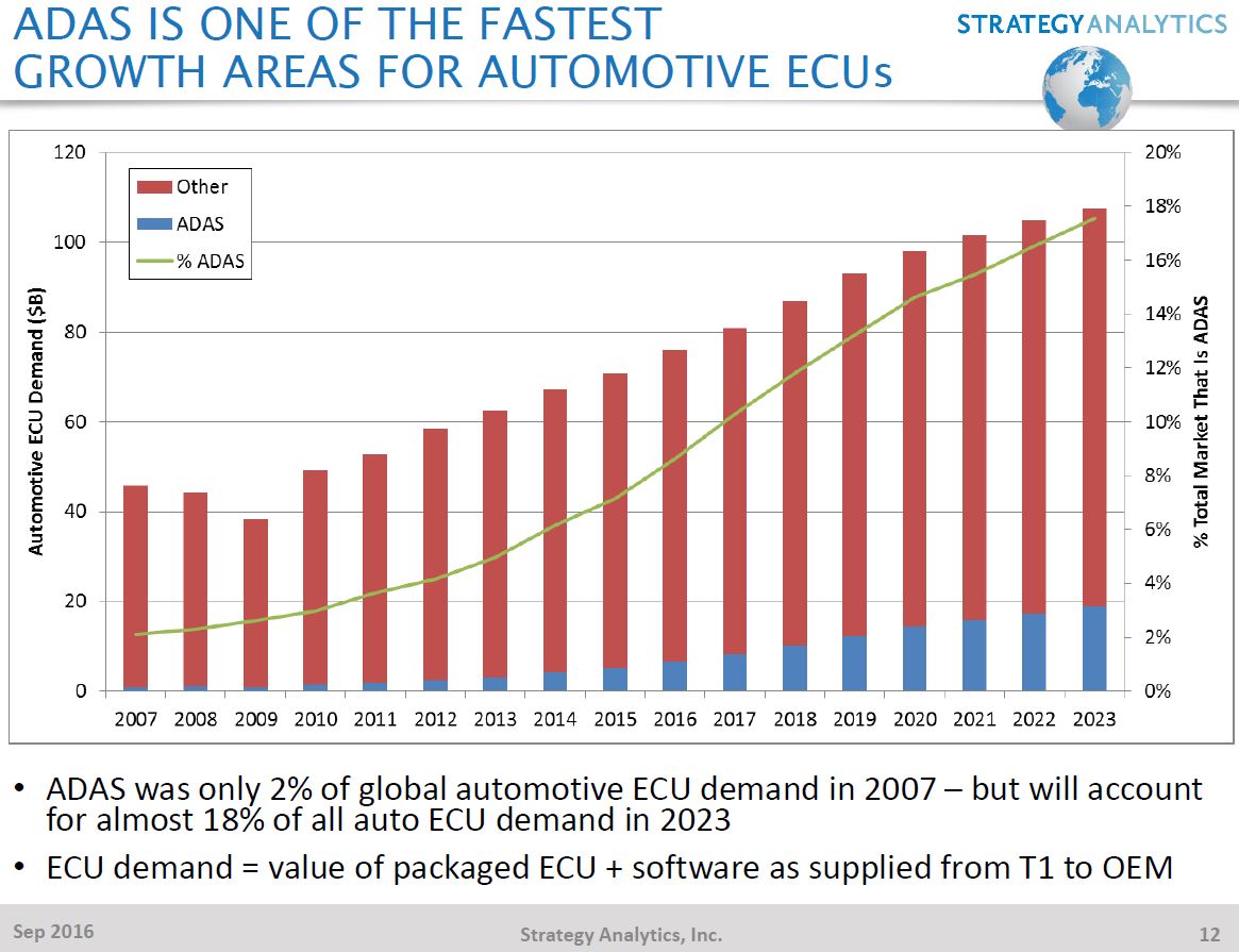
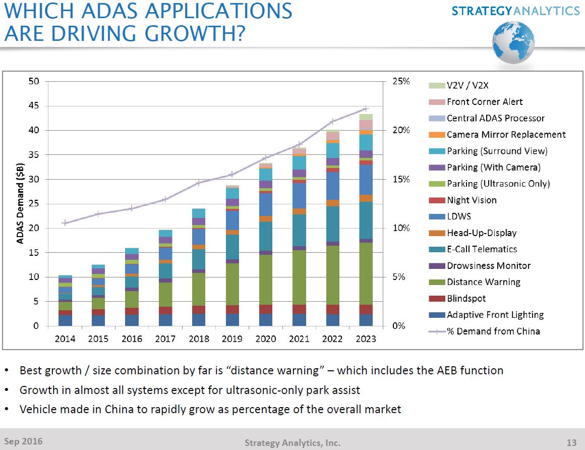
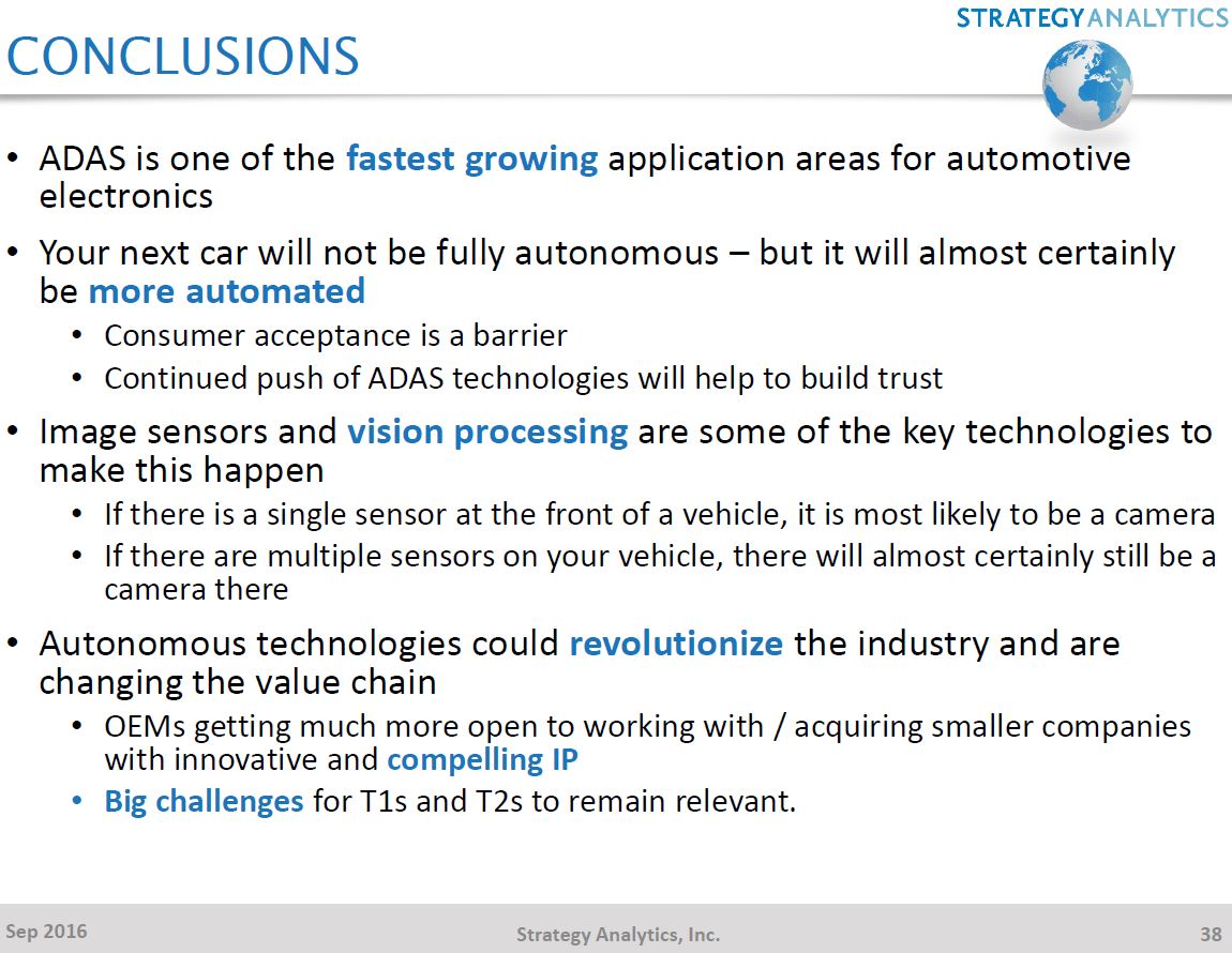
Strategy Analytics on ADAS Camera Market
Strategy Analytics presentation dated by Sept. 2016 forecasts a large growth for ADAS camera market:


Academic and University News
Prof. Shen Guozhen’s Group in Institute of Semiconductors, Chinese Academy of Sciences, with their collaborators in Hong Kong University of Science and Technology developed a flexible UV image sensor based on ZnO quantum dots (QDs) decorated ZTO nanowires (NWs). The device was fabricated on the flexible polyethylene terephthalate (PET) substrate, which displayed outstanding flexibility, electrical stability and folding endurance.
Duo to the rational band engineering at the QD/NW interface which results in effective separation of electron-hole pairs, the device showed ultrahigh specific detectivity (up to 9.0 × 10¹⁷ Jones), photoconductive gain (up to 1.1 × 10⁷) and high response speed (47 ms).

EETimes: Non-uniform spatial image sampling has been a popular idea over many decades. University of Glasgow, Scotland, UK, gives it another try in arxiv.org open-acess paper "Adaptive foveated single-pixel imaging with dynamic super-sampling" by David B. Phillips, Ming-Jie Sun, Jonathan M. Taylor, Matthew P. Edgar, Stephen M. Barnett, Graham G. Gibson, and Miles J. Padgett.
"In this work we take a different approach and adopt a strategy inspired by the foveated vision systems found in the animal kingdom - a framework that exploits the spatio-temporal redundancy present in many dynamic scenes. In our single-pixel imaging system a high-resolution foveal region follows motion within the scene, but unlike a simple zoom, every frame delivers new spatial information from across the entire field-of-view. Using this approach we demonstrate a four-fold reduction in the time taken to record the detail of rapidly evolving features, whilst simultaneously accumulating detail of more slowly evolving regions over several consecutive frames."

Friday, April 21, 2017
Reuters Says that Sony Image Sensors Cost is Lower than Expected
Reuters: Sony revises upward its annual profit estimation, in part due to the lower costs in its image sensor business. The official annual results for the company's fiscal year ended on March 31, 2017 are to be announced on April 28.
Samsung Galaxy S8 Rear Camera Teardown
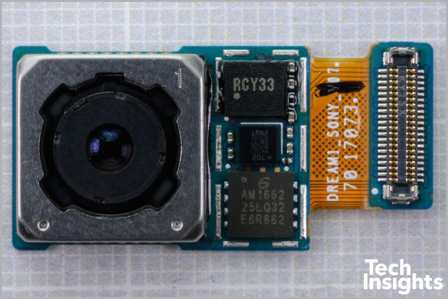
TechInsights posted a teardown info on Galaxy S8 rear camera. The 12MP stacked dual pixel image sensor has been identified as one made by Sony, probably IMX333. Other Galaxy S8 phones might contain Samsung-made sensors.
The absence of dual camera in a flagship phone is said to save about $12.50 from the final BOM costs for Samsung.


The absence of dual camera in a flagship phone is said to save about $12.50 from the final BOM costs for Samsung.

Analog Devices "Material Sensing Platform"
Analog Devices one more time demos its IR spectrometer-based Material Sensing Platform for smartphones, developed together with Consumer Physics. The previous demo is here.
Thursday, April 20, 2017
Samsung Galaxy S8 Teardown Reveals Stand-Alone ISP, Iris Scanner Internals
TechInsights publishes Samsung Galaxy S8 smartphone reverse engineering article listing Samsung S5C73C3 image processors among the other chips on the PCB. The front camera with iris scanner module is shown on the images below:
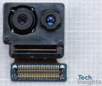


The front camera is based on Sony stacked IMX320, while the iris scanner BSI sensor is marked as S5K5E6YV (or S5K5E6YV). Both sensors have pixel pitch of 1.12um.


The front camera is based on Sony stacked IMX320, while the iris scanner BSI sensor is marked as S5K5E6YV (or S5K5E6YV). Both sensors have pixel pitch of 1.12um.
KAUST Interview with Eric Fossum
King Abdullah University of Science and Technology (KAUST), Saudi Arabia publishes an interview with Eric Fossum on CMOS sensor invention history and Quanta image sensor:
Wednesday, April 19, 2017
Mobileye CEO Demos Self-Driving Car
Mobileye CEO and Co-Founder Ziv Aviram demos his company self-driving car in the 360-deg surround video:
The full presentation at YPO Edge 2017 held in Vancouver, Canada can be seen here.
The full presentation at YPO Edge 2017 held in Vancouver, Canada can be seen here.
Sony Unveils Full-Frame Stacked Sensor
Sony presents a new A9 flagship full-frame ILC featuring 24MP stacked sensor. The stacking allows:
SonyAlphaRumors publishes a number of slides on the new image sensor:


- up to 20 fps speed,
- viewfinder or display blackout-free shooting,
- up to 60 AF/AE tracking calculations per second,
- silent vibration-free electronic shutter speeds up to 1/32000 sec.
- Anti-Distortion Shutter operation that minimizes distortion of moving subjects
- Full pixel array readout with no pixel binning for oversampled 4K 30p video
SonyAlphaRumors publishes a number of slides on the new image sensor:


Monday, April 17, 2017
Yole on Mobile Camera Trends
Yole Developpement publishes an article on mobile phone camera trends. Few quotes:
"First, it seems that in the recent years Apple has slowed down its innovation drive on the camera side, so competitors have been able to move ahead. This is the case for the dual camera setup on the rear side of the phones.
Second, the importance of biometry has had a direct impact on cameras, which are now potential biometric devices. Samsung has implemented a second front-side camera, in the same way Fujitsu had experimented with less than a year ago, in order to provide state of the art iris-recognition technology.
Third, the usage of the front camera is evolving quickly. We had mentioned in our CMOS Image Sensor report the selfie trend’s impact on front facing camera resolution. Companies like Oppo are surfing this wave by improving the performance of the front camera, and recently providing a dual front setup for the F3."

Yole on 3D Imaging Market
Yole Developpement releases report "3D Imaging and Sensing 2017." Few quotes from the flyer:
"In 2016 3D imaging & sensing devices became quite significant business wise, generating more than $1.3B in revenue. While Yole anticipated the advent of 3D imaging & sensing in consumer products by 2020, it seems the schedule has accelerated in recent months. 2018 will likely see a massive influx of products, with the first applications in mobile and computing. And with the iPhone8 expected to incorporate a front-facing 3D camera, 3D’s application as a user interface will finally be better understood. 3D imaging & sensing has made several consumer attempts in the past, i.e. the Kinect game accessory and the Leap motion gesture controller. This time around, we expect Apple to make it right and definitive. Augmented reality is an application, not hardware, and mobile will be the main benefactor of this innovation. Drones & Robots will also benefit from the situation. With a CAGR of 37.7% over the next five years, Yole Développement forecasts 3D imaging & sensing devices to reach $9B by 2022."
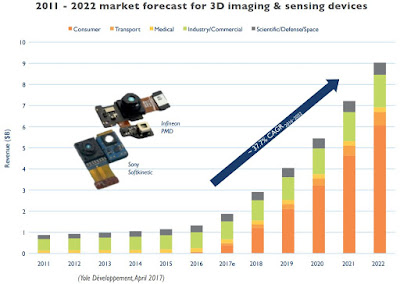

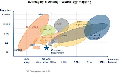
"In 2016 3D imaging & sensing devices became quite significant business wise, generating more than $1.3B in revenue. While Yole anticipated the advent of 3D imaging & sensing in consumer products by 2020, it seems the schedule has accelerated in recent months. 2018 will likely see a massive influx of products, with the first applications in mobile and computing. And with the iPhone8 expected to incorporate a front-facing 3D camera, 3D’s application as a user interface will finally be better understood. 3D imaging & sensing has made several consumer attempts in the past, i.e. the Kinect game accessory and the Leap motion gesture controller. This time around, we expect Apple to make it right and definitive. Augmented reality is an application, not hardware, and mobile will be the main benefactor of this innovation. Drones & Robots will also benefit from the situation. With a CAGR of 37.7% over the next five years, Yole Développement forecasts 3D imaging & sensing devices to reach $9B by 2022."


3D Imaging and AF Application Drive VSCEL Market
Yole Developpement IR light sources analysis shows that VCSEL market is set for a high growth due to wide adoption of 3D imaging and active ToF AF systems:


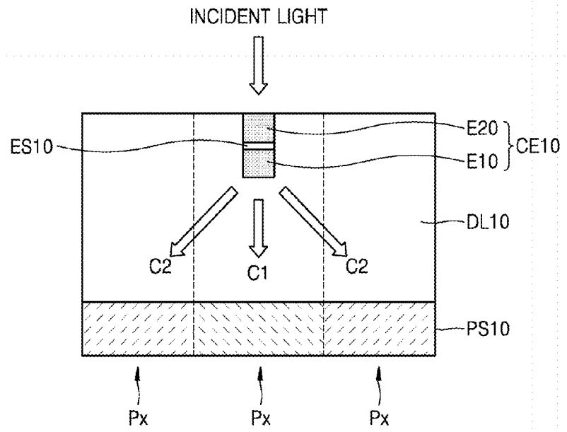
Samsung Files New Batch of Color Splitter Patent Applications
Samsung files another bunch of color splitter patent applications:
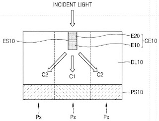
"The refractive index of the color splitter may be about 1.4 to about 2.4.
The color splitter may include one of high refraction index materials from the group consisting of SiNx, TiO2, ZnS, and ZnSe, or an optical polymer including nanoparticles of the high refraction index materials dispersed in the optical polymer."
- US20170098672 "Image sensor including color separation element" by Seokho Yun, Sookyoung Roh, Sunghyun Nam,
- US20170097510 "Image sensor and method of manufacturing the same" by Jinseung Sohn,
- US20170090206 "Color splitter structure, method of manufacturing the same, image sensor including color splitter structure, and optical apparatus including image sensor" by Ilhwan Kim, Doyoon Kim,
- US20170092668 "Optical apparatus including optical functional layer having high refractive index and method of manufacturing the optical apparatus" by Doyoon Kim, Ilhwan Kim.
- US20170092676 "Image sensor including color separation element and image pickup apparatus including the image sensor" by Seokho Yun, Sookyoung Roh, Sunghyun Nam
"The refractive index of the color splitter may be about 1.4 to about 2.4.
The color splitter may include one of high refraction index materials from the group consisting of SiNx, TiO2, ZnS, and ZnSe, or an optical polymer including nanoparticles of the high refraction index materials dispersed in the optical polymer."
Sunday, April 16, 2017
Algolux Presents its ISP Tuning Solution
Canadian startup company Algolux presents its ISP image quality tuning solution based on machine learning:
Saturday, April 15, 2017
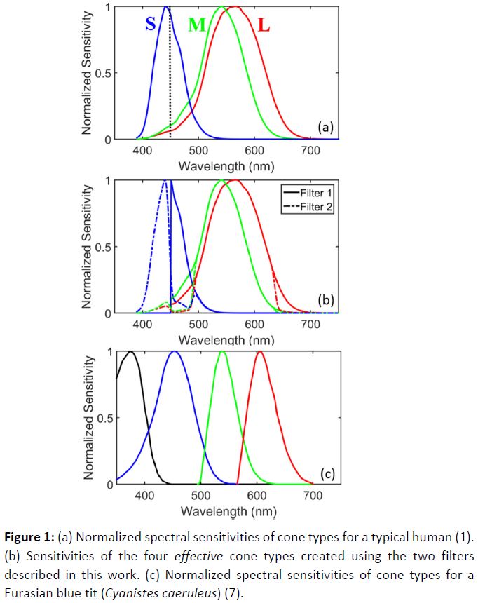
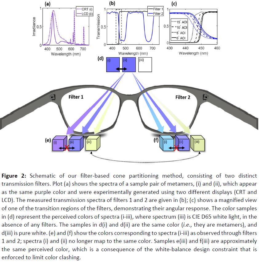
Human Color Vision Enhanced to 4 Colors
Electrons and Holes: University of Wisconsin-Madison researchers come up with an idea that potentially can kick-start a market for 4 or more color image sensors (and displays) instead of today's RGB ones. Their paper "Enhancement of human color vision by breaking the binocular redundancy" by Bradley S. Gundlach, Alireza Shahsafi, Gregory Vershbow, Chenghao Wan, Jad Salman, Bas Rokers, Laurent Lessard, and Mikhail A. Kats proposes a way to get some of the hyperspectral camera abilities in a very simple way:
"To see color, the human visual system combines the responses of three types of cone cells in the retina - a process that discards a significant amount of spectral information. We present an approach that can enhance human color vision by breaking the inherent redundancy in binocular vision, providing different spectral content to each eye. Using a psychophysical color model and thin-film optimization, we designed a wearable passive multispectral device that uses two distinct transmission filters, one for each eye, to enhance the user's ability to perceive spectral information. We fabricated and tested a design that "splits" the response of the short-wavelength cone of individuals with typical trichromatic vision, effectively simulating the presence of four distinct cone types between the two eyes ("tetrachromacy"). Users of this device were able to differentiate metamers (distinct spectra that resolve to the same perceived color in typical observers) without apparent adverse effects to vision. The increase in the number of effective cones from the typical three reduces the number of possible metamers that can be encountered, enhancing the ability to discriminate objects based on their emission, reflection, or transmission spectra. This technique represents a significant enhancement of the spectral perception of typical humans, and may have applications ranging from camouflage detection and anti-counterfeiting to art and data visualization."
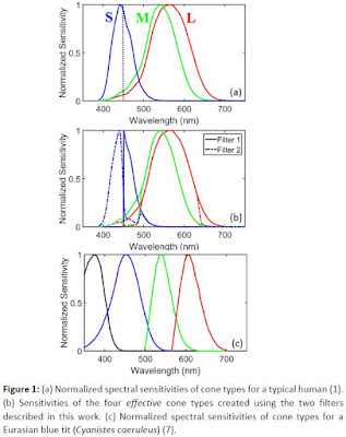

"To see color, the human visual system combines the responses of three types of cone cells in the retina - a process that discards a significant amount of spectral information. We present an approach that can enhance human color vision by breaking the inherent redundancy in binocular vision, providing different spectral content to each eye. Using a psychophysical color model and thin-film optimization, we designed a wearable passive multispectral device that uses two distinct transmission filters, one for each eye, to enhance the user's ability to perceive spectral information. We fabricated and tested a design that "splits" the response of the short-wavelength cone of individuals with typical trichromatic vision, effectively simulating the presence of four distinct cone types between the two eyes ("tetrachromacy"). Users of this device were able to differentiate metamers (distinct spectra that resolve to the same perceived color in typical observers) without apparent adverse effects to vision. The increase in the number of effective cones from the typical three reduces the number of possible metamers that can be encountered, enhancing the ability to discriminate objects based on their emission, reflection, or transmission spectra. This technique represents a significant enhancement of the spectral perception of typical humans, and may have applications ranging from camouflage detection and anti-counterfeiting to art and data visualization."
Thursday, April 13, 2017
Himax Invests in Emza Visual Sense
GlobeNewsWire: Himax makes a strategic investment in cash in exchange for a 45.1% equity ownership of Emza Visual Sense Ltd. (“Emza”), with a one-year option to acquire the remaining 54.9% of Emza’s equity and all outstanding stock options. Purchase price to acquire the remaining equity and all outstanding stock options of Emza if Himax elects to exercise the one-year option includes an all-cash initial purchase amount, along with earnout payments contingent on the performance of Emza. Terms of the investment were not disclosed.
Emza is an Israeli company developing a power-efficient visual sensors that include proprietary machine-vision algorithms and specific architectures that deliver always-on visual sensing capabilities, achieving orders of magnitude improvement in power consumption.
“This strategic investment in Emza compliments our previously announced ultra low power CMOS image sensor product and initiatives in delivering turn-key solutions for ‘always-on’ smart camera that enables devices capable of real-time contextual awareness, such as face detection and human presence detection and motion,” said Jordan Wu, CEO of Himax. “Together, we can transform our AoS sensor from a simple ‘image capturing device’ to an ‘information analytics device’ that offers significantly more value to our customers. This exciting new computer vision market demands highly efficient sensors, algorithms, camera and processor architectures capable of delivering extremely low power consumption in a small form factor so that it can be easily integrated into TVs and smartphones, as well as AR/VR, IoT, and AI devices.”
“Our partnership with Himax, who shares our vision of sub-milliwatt always-on visual sensors, provides Emza with access to a unique technology of ultra low-power CMOS and semi-conductors,” said Yoram Zylberberg, CEO of Emza. “Achieving the breakthrough of advanced computer vision at ultra low-power consumption requires tight integration between the silicon and algorithms. Our partnership with Himax gives us the opportunity to efficiently achieve and commercialize these breakthroughs.”
GlobeNewsWire: A week ago, Emza announced a partnership with DSP Group on low power vision processing. DSP Group is known by its low power always-on voice processors for smartphones ("OK Google"-type).
IISW 2017 Agenda
IISW to be held in Hiroshima, Japan on May 30-June 2, 2017 publishes its preliminary program. There are more than 100 image sensor papers, some of them quite surprising. Here are just some of the surprises:
Qualcomm works together with TSMC on a stacked image sensor design:
R02. A 3D Stacked Programmable Image Processing Engine in a 40nm Logic Process with a Detector Array in a 45nm CMOS Image Sensor Technologies
Biay‐Cheng Hseih, Keith Honea, Sami Khawam, Sergio Goma, RJ Lin, Chin‐Hao Chang, Charles Liu, Shang‐Fu Yeh, Hong‐Yi Tu, Kuo‐Yu Chou, Calvin Chao.
Qualcomm Technologies Inc. USA;
TSMC, Taiwan, ROC
Heptagon works with FBK on non-SPAD ToF image sensors with pinned PD and TG:
P22. Transfer-Gate Region Optimization and Pinned-Photodiode Shaping for High-Speed TOF Applications
Fabio Acerbi, Manuel Moreno Garcia, Gözen Köklü, Bernhard Buttgen, Radoslaw Gancarz, Alice Biber, Daniel Furrer, David Stoppa.
Fondazione Bruno Kessler, Center for Material and Microsystems, Italy;
Heptagon Advanced Micro Optics Pte Ltd., Switzerland
Brillnics publicly presents its technology, for the first time ever:
P29. Back Side Illuminated High Dynamic Range 3.0μm Pixel Featuring Vertical p-n Junction Capacitance in A Deep Pinned Photodiode
K. Mori, S.Okura, T. Hasegawa, S. Tanaka and I.Takayanagi.
Brillnics Japan Inc., Japan
Invisage comes up with a larger pixel sensor optimized for 940nm IR imaging:
R53. A QuantumFilm Based QuadVGA 1.5µm Pixel Image Sensor with Over 40% QE at 940 nm for Active Illumination Applications.
Nikolai Bock, Aurelien Bouvier, Dario Clocchiatti, Naveen Kolli, Vitanshu Sharma, Emanuele Mandelli.
InVisage Technologies, USA
Wednesday, April 12, 2017
Dark Current Blooming
ISAE, CEA and Toulouse University publish a paper on an well known but rarely discussed effect of "Dark Current Blooming in Pinned Photodiode CMOS Image Sensors" by Jean-Marc Belloir, Jean-Baptiste Lincelles, Alice Pelamatti, Clémentine Durnez, Vincent Goiffon, Cédric Virmontois, Philippe Paillet, Pierre Magnan, Member, and Olivier Gilard, also available at IEEE TED.
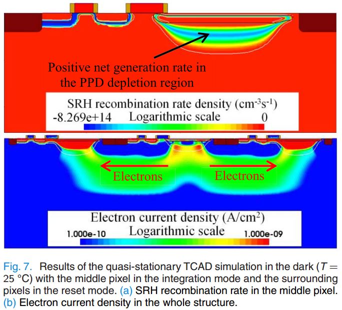
"This paper demonstrates the existence of dark current blooming in pinned photodiode (PPD) CMOS image sensors (CISs) with the support of both experimental measurements and TCAD simulations. It is usually assumed that blooming can appear only under illumination, when the charge collected by a pixel exceeds the full well capacity (FWC) (i.e., when the photodiode becomes forward biased). In this paper, it is shown that blooming can also appear in the dark by dark current leakage from hot pixels in reverse bias (i.e., below the FWC). The dark current blooming is observed to propagate up to nine pixels away in the experimental images and can impact hundreds of pixels around each hot pixel. Hence, it can be a major image quality issue for the state-of-the-art PPD CISs used in dark current limited applications, such as low-light optical imaging and should be considered in the dark current subtraction process. This paper also demonstrates that one of the key parameter for dark current optimization, the transfer gate bias during integration, has to be carefully chosen depending on the application because the optimum bias for dark current reduction leads to the largest dark current blooming effects."


"The effect of the TG bias (VTG) during integration on the dark current blooming has been investigated (Fig. 9). A slight negative bias (−0.2 V in this paper) is usually chosen for low-light imaging because it ensures a very low mean dark current of the CIS. Indeed, the oxide interface under the TG is mainly accumulated with holes in that case, which neutralize the interface generation centers [15]. However, the potential barrier under the TG is higher than the potential barrier between the PPD and the epitaxy, because the substrate is grounded (0 V). Therefore, the dark current of the PPD is rather emitted toward the epitaxy than under the TG by thermionic emission, which leads to the dark current blooming (Fig. 9). If the TG is biased positively (+0.2 V in Fig. 9), which is a common light induced blooming countermeasure, the potential barrier under the TG becomes lower than toward the epitaxy and the dark current will rather diffuse under the TG (and will be collected by the floating diffusion) than toward the epitaxy. In that case, it can be seen in Fig. 9 that the dark current blooming is supressed. However, the mean dark current of the CIS is higher due to the depleted oxide interface under the TG."

"This paper demonstrates the existence of dark current blooming in pinned photodiode (PPD) CMOS image sensors (CISs) with the support of both experimental measurements and TCAD simulations. It is usually assumed that blooming can appear only under illumination, when the charge collected by a pixel exceeds the full well capacity (FWC) (i.e., when the photodiode becomes forward biased). In this paper, it is shown that blooming can also appear in the dark by dark current leakage from hot pixels in reverse bias (i.e., below the FWC). The dark current blooming is observed to propagate up to nine pixels away in the experimental images and can impact hundreds of pixels around each hot pixel. Hence, it can be a major image quality issue for the state-of-the-art PPD CISs used in dark current limited applications, such as low-light optical imaging and should be considered in the dark current subtraction process. This paper also demonstrates that one of the key parameter for dark current optimization, the transfer gate bias during integration, has to be carefully chosen depending on the application because the optimum bias for dark current reduction leads to the largest dark current blooming effects."
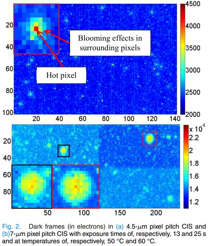
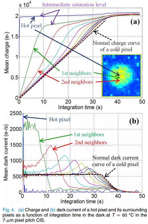
"The effect of the TG bias (VTG) during integration on the dark current blooming has been investigated (Fig. 9). A slight negative bias (−0.2 V in this paper) is usually chosen for low-light imaging because it ensures a very low mean dark current of the CIS. Indeed, the oxide interface under the TG is mainly accumulated with holes in that case, which neutralize the interface generation centers [15]. However, the potential barrier under the TG is higher than the potential barrier between the PPD and the epitaxy, because the substrate is grounded (0 V). Therefore, the dark current of the PPD is rather emitted toward the epitaxy than under the TG by thermionic emission, which leads to the dark current blooming (Fig. 9). If the TG is biased positively (+0.2 V in Fig. 9), which is a common light induced blooming countermeasure, the potential barrier under the TG becomes lower than toward the epitaxy and the dark current will rather diffuse under the TG (and will be collected by the floating diffusion) than toward the epitaxy. In that case, it can be seen in Fig. 9 that the dark current blooming is supressed. However, the mean dark current of the CIS is higher due to the depleted oxide interface under the TG."

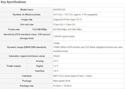
Sony Unveils Automotive HDR Sensor with LED Flicker Reduction
PRNewswire: Sony announces a 2.45MP 1/2.7-inch CMOS sensor for automotive cameras, the IMX390CQV. Sony will begin shipping samples in May 2017.
The new image sensor features an LED flicker mitigation function that reduces flickering when shooting LED signs and traffic signals, as well as an HDR of 120dB (measured according to EMVA1288). The IMX390CQV is said to be the first in the industry that can simultaneously mitigate LED flicker and shoot in HDR, made possible by Sony's new pixel structure and exposure method. It also offers high-sensitivity down to 0.1 lux.
Sony publishes two Youtube videos demoing the LED flicker reduction and HDR features:


The IMX390CQV is planned to meet the requirements of the AEC-Q100 Grade 2 automotive electronic component reliability tests this fiscal year. Moreover, with this new product, Sony also introduced a development process that complies with ISO26262 automobile functional safety standards, aiming to achieve a high level of design quality for an automotive product. The new sensor also meets the functional safety requirement level ASIL C.
Thanks to DS for the pointer!
The new image sensor features an LED flicker mitigation function that reduces flickering when shooting LED signs and traffic signals, as well as an HDR of 120dB (measured according to EMVA1288). The IMX390CQV is said to be the first in the industry that can simultaneously mitigate LED flicker and shoot in HDR, made possible by Sony's new pixel structure and exposure method. It also offers high-sensitivity down to 0.1 lux.
Sony publishes two Youtube videos demoing the LED flicker reduction and HDR features:


The IMX390CQV is planned to meet the requirements of the AEC-Q100 Grade 2 automotive electronic component reliability tests this fiscal year. Moreover, with this new product, Sony also introduced a development process that complies with ISO26262 automobile functional safety standards, aiming to achieve a high level of design quality for an automotive product. The new sensor also meets the functional safety requirement level ASIL C.

Thanks to DS for the pointer!
Tuesday, April 11, 2017
Mediatek Brags About 10-Frame Fast PDAF+AE+WB with Helio X30 SoC
Mediatek publishes a X30 processor presentation video claiming it's able to achieve PDaf, AE and WB in just 10 frames. The only unknown here is the frame rate during the the PDAF, AE and WB stage.
The Helio X30 SoC camera features:
Imagiq 2.0 ISP
The Helio X30 SoC camera features:
Imagiq 2.0 ISP
- Two 14-bit ISPs supporting 16+16MP dual camera functionality allows such as wide+zoom combination lenses allow real-time depth of field effects, fastest auto exposure, improved real-time denoise in low-light conditions.
- Vision Processing Unit
- Programmability and Flexibility: The VPU provides a platform that allows brands the ability to customize camera functionality and drive product differentiation.
- Huge Power Reduction: The VPU is a dedicated camera-assisting hardware unit it has the ability to perform real-time processing functions, that were typically assigned to CPU or GPU, with only 1/10th power usage.
- Performance Boost: The VPU can still be used in isolation or as part of a team with the CPU/GPU, employing heterogeneous computing on same memory subsystem for advanced system or multi-application/function tasks.
- 4K HDR Video
- ClearZoom and Temporal Noise Reduction (TNR) technologies enable a sharp, crisp digital zoom up to 10x magnification.
- Works for both video and photography.
- Miravision EnergySmart Screen
- The dedicated Camera Control Unit (CCU) hardware delivers considerably faster, automatic exposure adjustment when environmental lighting conditions change suddenly. AE convergence speed is up to twice as fast as competitive auto exposure performance.
- Access to MediaTek’s deep learning SDK featuring support for Caffe and Google’s TensorFlow frameworks, opening up the latest in machine intelligence to developers.
ON Semi Expands EMCCD Product Range
BusinessWire: ON Semi is expanding its portfolio of IT-EMCCDs to target not only low-light industrial applications such as medical and scientific imaging, but also commercial and military applications for high-end surveillance.
The new 4MP KAE-04471 uses larger 7.4um pixels than those found in existing IT-EMCCD devices, doubling the light gathering capability of the new device and improving image quality under light starved conditions. The KAE-04471 is pin and package compatible with the existing 8MP KAE-08151.
The new KAE-02152 shares the same 1080p resolution and 2/3” optical format as the existing KAE-02150, but incorporates an enhanced pixel design that increases sensitivity in NIR band – an improvement that can be critical in applications such as surveillance, microscopy and ophthalmology. The KAE-02152 is fully drop-in compatible with the existing KAE-02150, and both devices are available in packages that incorporate an integrated thermoelectric cooler, simplifying the work required by camera manufacturers to develop a cooled camera design.
“As the need for sub-lux imaging solutions expands in surveillance, medical, scientific and defense markets, customers are looking for new options that provide the critical performance required in these applications,” said Herb Erhardt, VP and GM, Industrial Solutions Division, Image Sensor Group at ON Semiconductor. “The new products allow customers to choose from a variety of resolutions, pixel sizes, sensitivities, color configurations and packaging options in our IT-EMCCD portfolio to meet their low-light imaging needs.”
An intra−scene switchable gain feature samples each charge packet on a pixel−by−pixel basis, enabling the camera system to determine whether the charge will be routed through the normal gain output or the EMCCD output based on a user selectable threshold. This feature is said to enable imaging in extreme low light even when bright objects are within a dark scene, allowing a single camera to capture quality images from sunlight to starlight.
Engineering grade versions of the KAE-04471 are now available, with production versions available in 2Q17. Engineering grade versions of the KAE-02152 in both a standard package as well as a package incorporating an integrated thermoelectric cooler are also available, with production versions of both configurations available in 3Q17. All IT-EMCCD devices ship in ceramic micro-PGA packages, and are available in both Monochrome and Bayer Color configurations.
Update: ON Semi also published a webcast explaining its IT-EMCCD technology:
The new 4MP KAE-04471 uses larger 7.4um pixels than those found in existing IT-EMCCD devices, doubling the light gathering capability of the new device and improving image quality under light starved conditions. The KAE-04471 is pin and package compatible with the existing 8MP KAE-08151.
The new KAE-02152 shares the same 1080p resolution and 2/3” optical format as the existing KAE-02150, but incorporates an enhanced pixel design that increases sensitivity in NIR band – an improvement that can be critical in applications such as surveillance, microscopy and ophthalmology. The KAE-02152 is fully drop-in compatible with the existing KAE-02150, and both devices are available in packages that incorporate an integrated thermoelectric cooler, simplifying the work required by camera manufacturers to develop a cooled camera design.
“As the need for sub-lux imaging solutions expands in surveillance, medical, scientific and defense markets, customers are looking for new options that provide the critical performance required in these applications,” said Herb Erhardt, VP and GM, Industrial Solutions Division, Image Sensor Group at ON Semiconductor. “The new products allow customers to choose from a variety of resolutions, pixel sizes, sensitivities, color configurations and packaging options in our IT-EMCCD portfolio to meet their low-light imaging needs.”
An intra−scene switchable gain feature samples each charge packet on a pixel−by−pixel basis, enabling the camera system to determine whether the charge will be routed through the normal gain output or the EMCCD output based on a user selectable threshold. This feature is said to enable imaging in extreme low light even when bright objects are within a dark scene, allowing a single camera to capture quality images from sunlight to starlight.
Engineering grade versions of the KAE-04471 are now available, with production versions available in 2Q17. Engineering grade versions of the KAE-02152 in both a standard package as well as a package incorporating an integrated thermoelectric cooler are also available, with production versions of both configurations available in 3Q17. All IT-EMCCD devices ship in ceramic micro-PGA packages, and are available in both Monochrome and Bayer Color configurations.
 |
| KAE-04471 Spec |
 |
| KAE-02152 Spec |
Update: ON Semi also published a webcast explaining its IT-EMCCD technology:
Subscribe to:
Posts (Atom)