As Ren Ng posted in Lytro company blog, "we have entered a new chapter for Lytro. I have decided to step aside as CEO and take on a new role that will let me concentrate on innovation as Executive Chairman. I will remain a full-time employee, 100% focused on Lytro. In my new role I will shift attention from day-to-day operations, to focus again on product vision, technology, and strategic direction for the company.
Charles Chi will be taking over as interim CEO. Charles has been our Executive Chairman for the last two years."
"The last two years have been a very exciting and dramatic period of growth for Lytro. We launched the company out of stealth, raised approximately $50M, grew a team of over 80 people, and shipped a truly revolutionary product."
Some time ago Banpil came with a bold statement of knowing a way to build broad spectrum imagers, claimed "to be manufactured by using conventional semiconductor process":
Now Banpil says that the patents on this technology have have been granted. While the company does not give the patent numbers, it appears to be US8174059 and US8101971 patents, offering a stack of InGaAs photoabsorption layer on GaAs or InP substrate:
The photodiode has n type InP substrate 10, n+ and low doped InAs(y)P(1-y) buffer layers 11, InAs(0.6)P(0.4) layer 13, In(0.8)Ga(0.2)As layer 15 as absorption layer, highly doped InAs(0.6)P(0.4) layer 17 for ohmic contact. Photodiode has the n type ohmic contact 20 at the backside of the substrate 10, and p type of ohmic contact 22 at the top of the photodiode.
The patent's abstracts sound almost like an ad: "Novel structures of the photodetector having broad spectral ranges detection capability are provided. The photodetector offers high quantum efficiency >95% over wide spectral ranges, high frequency response >10 GHz (@3 dB). The photodiode array of N x N (or M x N) elements is also provided. The array also offers wide spectral detection ranges ultraviolet to 2500 nm with high quantum efficiency >95% and high frequency response of >10 GHz, cross-talk of <0.1%. In the array, each photodiode is independently addressable and is made either as top-illuminated or as bottom illuminated type detector. The photodiode and its array provided in this invention, could be used in multiple purpose applications such as telecommunication, imaging, and sensing applications including surveillance, satellite tracking, advanced lidar systems, etc. The advantages of this photodetectors are that they are uncooled and performance will not be degraded under wide range of temperature variation."
Banpil has made sample-level sensor array products available for demonstration by request.
Leti Annual Research Report 2011 too presents multispectral imagers based on n on
p photodiodes implanted in a thin HgCdTe film (few μm) grown on CdZnTe substrate (see p. 15). Leti managed to extend their spectral response from the usual LWIR band all the way to 250nm UV:
On p. 36 Leti presents its work on Fabry-Perot RGB filters with nice looking color separation graphs, sans somewhat low peak transmission:
Truesense Imaging blog says that the four camera systems on Mars rover Curiosity are all based on the Truesense Imaging KAI-2020 image sensor. The Mars Descent Imager (MARDI) will capture images during descent to provide a framework of the landing site for early operations, while the Mars Hand Lens Imager (MAHLI) will capture high resolution images (up to 14.5 μm per pixel) of Martian rocks and soil after landing. And the Mast Camera (MastCam) includes two cameras – each with the same sensor but using different lenses – that will capture high resolution still and 720p video images of the planet’s surface. And all of them rely on the KAI-2020 to capture full color, high resolution images.
Curiosity is scheduled to land on Mars on August 6, 2012.
Albert Theuwissen continues his "How to Measure..." series of articles. The last one on temporal noise in darkness discusses the procedure and the results interpretations.
EE Journal: CMOSIS announces a 20MP global shutter sensor for industrial applications. The new CMV20000 sensor features 5,120 x 3,840 resolution with 6.4 um sized pixels resulting in an active sensor area of 32.8 x 24.6 mm (35 mm film optical format). Its peak QE is more than 45%, responsivity is 8.29 V/lux.s, and DR is 66 dB. The 8T pixel is said to reduce dark noise and FPN of the sensor.
At full 20MP resolution and with a 12-bit ADC resolution the CMV20000 delivers 30 fps. This is achieved by using 16 LVDS outputs running at 480 Mbit/s each. At full resolution and frame rate, the power dissipation is 1.1W. This power consumption can be dynamically controlled when lower frame rates are used.
Driving and programming the on-chip features such as HDR modes, offset and gain programming and power dissipation control is done over a 3-wire read-write SPI control.
The monochrome variant of the CMV20000 sensor is in production today. A color variant, with RGB Bayer CFA filter, will be introduced to the market in Q4 2012. It is housed in a ceramic 143-pin PGA package and can be operated in the -20 to +70 ºC temperature range.
The CMV20000 was originally developed as a customized, exclusive product aimed at complex traffic management applications. An agreement with the original customer allows CMOSIS to offer this imager to third parties for applications outside the traffic field.
Marketwire: InVisage announces that it has named industry veteran Syrus P. Madavi as chairman of the board. In addition to his position as chairman of InVisage, Madavi is president of a private fund SPM Capital. Madavi's career has included serving as chairman, president and CEO of Burr-Brown Corporation; president, COO, and director of JDS Uniphase; SVP of TI; president of Raytheon Semiconductor; and founder and president of Signal Processing Technologies.
Sony PR: Sony announces its plans to invest in its Nagasaki Technology Center ("Nagasaki TEC") from the first half of the fiscal year ending March 31, 2013 through the first half of the fiscal year ending March 31, 2014, to increase the production capacity for stacked CMOS sensors, aimed mainly to smartphones.
This investment is intended to provide for new wafer processing equipment for stacked CMOS image sensors, and to increase and transform wafer lines capable of manufacturing CMOS image sensors. With this development, Sony plans to increase total production capacity for CCD and CMOS image sensors to approximately 60,000 of 300mm wafers per month by the end of September 2013.
The investment amount is approximately 80 billion yen ($997M), of which, the amount to be invested in the current fiscal year ending March 31, 2013 (approximately 45 billion yen) was included in the forecast of the capital expenditures for semiconductors in the current fiscal year announced at the annual earnings release on May 10, 2012. In addition, Sony will utilize a governmental subsidy in its investment plan which will be provided by the Ministry of Economy, Trade and Industry in Japan, through the "Subsidy for Domestic Location Promotion Projects" program.
Mobile sensors trend is a pixel shrink while maintaining the performance by advanced processing, such as BSI, new color filters, etc.:
Pixel and process evolution in Samsung
Sensitivity trend versus pixel size
(a) light loss ratio at each component
(b) spectral response of Samsung 6th and 7th generation CF
Camera module temperature vs power density for CIS SOC type
Not that much said about DSC trends. DSLR sensors use 130nm and 180nm process and, possibly, offer global shutter in future. Automotive sensor adoption is expected to be driven by many safety laws:
Laws and regulations affecting the in-car camera market, by TSR 2011
In the end paper talks about different automotive interfaces and importance of HDR. All in all, it's quite interesting and easy read targeted to wide audience.
Zolmax News: JPMorgan analysts wrote: "Omnivision’s move to 12-inch 65nm BSI-2 product is still a work in progress, which might explain management’s circumspect commentary on the recent earnings call. We remain constructive regarding the firm’s late 2012 through 2013 prospects, but we are incrementally cautious with a near-term perspective."
All Things D: Facebook has acquired facial recognition technology company Face.com, reportedly for $60M. Face.com's iPhone KLIC application automatically identifies and tags Facebook friends in photos. By connecting with Facebook, the app scans friends' photos to develop a facial profile of everyone in a user's network. The app identifies people by matching faces in photos taken with, or uploaded to, the app to these profiles. The company says KLiK is approximately 90% accurate (Reuters).
The company also provides technology that reveals gender, mood, and even age. "We provide a minimum and maximum and approximate age guesstimate, only using the facial information in the photo -- nothing else," Face.com CEO Gil Hirsch said.
Discovery News, Nature Journal: A group led by David Brady, EE professor at Duke's Pratt School of Engineering with scientists from the University of Arizona (UA), UCSD, and Distant Focus Corp. developed a Gigapixel camera named AWARE-2. The camera is said to use 98 microcameras, each with a 14MP sensor, grouped around a shared spherical lens. Together, they take in a field of view 120 degrees wide and 50 degrees tall. With all the packaging, data-processing electronics and cooling systems, the entire camera is about 0.75 by 0.75 by 0.5 metres in volume. 97% of the physical camera is comprised of the electronics and computer; only about 3% is devoted to the optical elements.
A one-gigapixel image (top) shows minute details (bottom) of the skyline
in Seattle, Washington
Business Wire: Science and Technology Facilities Council’s (STFC) Rutherford Appleton Laboratory (RAL) and TowerJazz have developed 120mm x 145mm X-Ray sensor wich is said to effectively use an entire 200mm wafer. The sensor's focal plane has a size of 139.2 x 120 mm, and has 6.7MP resolution (2800 x 2400 format) with a 50um pixel pitch, 32 analog outputs and also features low noise, a high DR and a programmable region-of-interest readout. Each 3T pixel has low-noise partially pinned photodiode, offering ‘charge-binning’ capability. The sensor offers a very high frame rate of 40fps at full resolution and ‘binned’ images can be read at an increasingly faster rate.
The device has sensing pixels right up to the edges on three sides of the imager. This allows multiple sensors, manufactured on cost-effective 200 mm silicon wafers, to be ‘butted’ or ‘tiled’ together in a 2 x 2 arrangement to form a significantly larger imaging area and to meet the requirements for mammography applications. Additionally, any 2 x N sensor arrangements are possible, thus making the device ideal for applications that demand even larger area coverage, such as chest imaging or security scans.
Tanner is also announcing that the project relied exclusively on its tools.
I've not seen it published in open access before, even though the data was available for quite a some time. Part of the data has been presented at IISW 2011. Fujifilm USA presents its materials for the color filters.
5th generation RGB CFA, suitable for 1.75um and bigger pixels
4th generation CMY CFA, suitable for 2um and bigger pixels
Nokia continues to invest in its imaging technologies and announces its intention "to acquire world-class imaging specialists as well as all technologies and intellectual property from Scalado AB".
"Nokia has been working with Scalado for more than ten years and they've contributed to many of our leading imaging applications," said Jo Harlow, executive vice president, Smart Devices at Nokia. "This transaction would enable us to combine our leadership in camera devices with their expertise in imaging, helping people move beyond taking pictures to capturing moments and emotions and then reliving them in many different ways." A Youtube video below demos Scalado Rewind, one of these many ways:
Recently announced Scalado Photobeamer allows instant viewing of photos by pointing the iPhone on any screen displaying www.photobeamer.com site, without any needs for pre-configurations or pre-registrations:
The acquisition is expected to close during the third quarter of 2012. The terms of the acquisition are confidential.
Founded in 2000 in Lund, Sweden, Scalado has more than 50 patent and patent pending technologies. Scalado technologies are in over 1 billion mobile devices, a figure growing with over 500 million each year. The company already licenses its solutions to the top five tier 1 mobile phone manufacturers, top 10 ISP/Sensor companies, and most leading platform providers. Customers/partners include Sony Ericsson, Nokia, Motorola, HTC, LGE, Samsung, NEC, Aptina, OmniVision, Fujitsu, Renesas, Qualcomm and MediaTek.
EDN published large 2-part article on image sensors for embedded vision systems. 6-page Part 1 is titled "Image sensors evolve to meet emerging embedded vision needs" and is written by Embedded Vision Alliance editor-in-chief Brian Dipert and his colleagues Eric Gregori and Shehrzad Qureshi. In a very popular form it describes automotive, mobile and regular cameras, 3D imaging and light field cameras.
The second part is devoted to HDR imaging and is written by Michael Tusch, CEO of Apical. Talking about various HDR implementations, the article describes Altasens' 1080p/60 A3372 sensor using a "checkerboard" pixel structure, wherein alternating Bayer pattern (RGGB) quad-pixel clusters are set to long- and short-exposure configurations:
"Long exposure delivers improved signal-to-noise but results in the saturation of pixels corresponding to bright details; the short exposure pixels conversely capture the bright details properly. Dynamic range reaches ~100 dB. The cost of HDR in this case is the heavy processing required to convert the checkerboard pattern to a normal linear Bayer pattern. This reconstruction requires complex interpolation because, for example, in highlight regions of an HDR image, half of the pixels are missing (clipped). An algorithm must estimate these missing values.
While such interpolation can occur with remarkable effectiveness, some impact on effective resolution inevitably remains. However, this tradeoff is rather well controlled, since the sensor only needs to employ the dual-exposure mode when the scene demands it; the A3372 reverts to non-HDR mode when it's possible to capture the scene via the standard 12-bit single-exposure model."
Update: Another version of this article is published by EDN-Europe on Oct. 1, 2012.
I missed this news from three weeks ago that Microsoft and LG CNC are to jointly develop “Gesture Recognition-based” solutions.
On May 22, LG CNS CEO Daehoon Kim had a meeting with Microsoft CEO Steve Ballmer, Tracey Fellows, VP of the Asia Pacific Region for Microsoft, and MS Korea CEO James Kim at COEX Inter-Continental Hotel in Seoul, Korea. The top management of the two companies held discussions on entry into the global market through joint development of "gesture recognition-based solutions".
LG CNS is to develop solutions with new NUI technology by Microsoft in the fields of smart media and smart factory. For instance, NUI can be used to control TV via voice and gestures and receive content and ad service tailored to your viewing pattern.
From right to left: LG CNS CEO Daehoon Kim, MS CEO
Steve Ballmer, and MS Korea CEO James Kim.
AnaFocus presents the LINCE5M high-speed 5.2MP CMOS sensor for machine vision and intelligent transportation systems.
The sensor array utilizes pixels with pinned photodiodes. The pixel response can be configured for either linear one with 61dB or for HDR piecewise linear response with more than 100dB DR; both with global shutter operation.
Truesense Imaging blog talks about the changes in the company life since it became independent. Basically, everything remains the same, except the name and logo switch on the buildings, business cards, documents, etc.
MacRumors quote KGI Securities analyst Ming-Chi Kuo saying:
"[A] number of components have required a slim-down. The component that will undergo the most dramatic make-over is the rear camera. Our research shows that iPhone 5 will feature the first-ever slimmed rear camera of all iPhones, in an effort to deliver an ultra-slim iPhone 5.
Meanwhile, to enhance photography effects, iPhone 5’s rear camera will feature a larger f/2.2 aperture than iPhone 4S’s f/2.4. However, larger aperture means more noises. In addition, the reduced thickness means even greater challenges for lens design and assembly, as not only the lens, but also the voice coil motor (VCM) and CMOS image sensor (CIS) need to be slimmer. Finally, the compact camera module (CCM) suppler, responsible for the terminal assembly, will be confronted by assembly yield."
Other Kuo's statements are:
The front-facing camera will be HD instead of the current VGA
The front-facing camera adopts new flip-chip package to reduce its thickness
Engadget, Hexus: SoftKinetic announces what it calls the world's smallest HD gesture recognition camera. The DepthSense 325 (DS325) is a pocket-sized camera that sees both in 3D (depth) and HD 2D (color). The DS325 can operate from as close as 10cm and includes a high-resolution depth sensor with a wide field of view, combined with HD video and dual microphones. The DS325 Professional Kit is available for pre-order now at SoftKinetic's online store at $249 with worldwide shipping included and is expected to begin shipping in the coming weeks.
A Youtube video from Taipei, Taiwan Computex shows the new camera in action:
SDM-WDM indoor optical wireless LAN using dedicated CMOS image sensors.
The prototype sensor is made in 0.35um process and has resolution of 64 x 64 100um pixels. A per-pixel bandwidth is 7.9MHz (simulation). The prototype system achieved speed of 10Mbps. The next generation sensor in 0.18um process is planned to have 180x84 pixels providing >1Gbps speed in the system.
At first I was surprised to see the low noise is required for a sun sensor. Most of this was answered in section discussing the algorithms and sun tracking camera design.
All-Electronics.de interviewed Jochen Hanebeck, president of the Automotive Division of Infineon Technologies. As Google translation states, Jochen presented:
"A world first is our 3D camera chip with 100,000 pixels, which is the result of cooperation with the firm of PMD. In principle, this sensor sends out infrared light and measures the return stroke, the phase shift. It delivers to each pixel so that not only a 2D but additionally a depth information. Other important characteristics are low latency and high frame rates of up to 100 frames/s at a very small form factor.
We have taken up the cause, enhance sensitivity and performance of this imager to significantly further and integrate. The use of high performance A/D converters on the chip we already deliver digital signals at the output.
Our 3D chip covers the entire area of interest to about 50 feet away. Due to the active illumination of an infrared LED array, the system has a night vision capability, so that is possible even in the dark a pedestrian and a gesture recognition controller. Vehicles with this technology could already from 2014 the production line."
Jochen Hanebeck shows the new 3D imager. The picture
was taken with such an imager. Depending on the distance
from the camera the colors vary from red (close) through
yellow and green to blue (away). (Source: Infineon
Technologies)
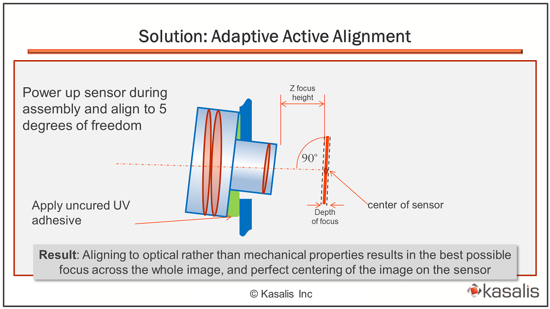
Kasalis (Burlington, MA) launches its first two products of active alignment of camera modules, the Pixid 100 R&D and the Pixid 100 Pro. The active alignment relies on the camera image during the final tuning process:
While the full system lineup is quite broad, only Pixid 100 R&D and the Pixid 100 Pro are available for shipment now:
Pixid 100 R&D Camera Module Alignment System
Kasalis was founded in 2011. It has completed its second round of investment in February 2012. The investment round is a private placement and details were not disclosed at the time.
PR Newswire: Singapore A*STAR Institute of Microelectronics (IME) and UMC have agreed to develop TSV technology for BSI CMOS sensors.
Leveraging on IME's 300mm TSV line which features advanced capabilities in TSV wafer thinning, bonding, redistribution layer (RDL) and bumping, this project will develop a TSV process for integration with the CIS device. The project targets higher performance applications, including next generation high resolution SLR cameras and camcorders, as well as smartphones, digital cameras and tablet computers.
"IME continues to enjoy a successful partnership with UMC and remains committed to innovation and cutting-edge technology development to help UMC quickly capture new growth opportunities," commented Professor Dim-Lee Kwong, Executive Director of IME.
Po Wen Yen, SVP at UMC, added, "We are delighted to expand our relationship with IME for BSI technology using TSV. IME's capabilities and expertise in TSV integration will complement UMC's successful efforts for via-middle and via-last TSV on standard 28nm CMOS, and will be a valuable asset to help us extend our market and technology leadership in CMOS image sensor."
Omnivision's patent application US20120113306 proposes to increase the sensor's speed by pipelining the readout and ADC circuits, so that the next pixel output can be read while column ADC processes the previous sample. To me, the idea is quite obvious and was used in sensors well before the priority date of Nov. 2010:
Photonics.com published e2v article "Quantum Efficiency Advances Sensors for Night Vision" by Frederic DeVriere, marketing manager for aerospace and defense imaging at e2v in Grenoble, France. The mentioned sensors are electron-bombardment CMOS and CCD for use with image intensifiers, EMCCDs and the new e2v Ruby series with enhanced IR response.
Albert Theuwissen continues his excellent series of "How to Measure..." articles. The latest one talks about temporal noise in dark, its sources, measurement and interpretations.
Transparency Market Research released an unusual image sensor market report named "Image Sensors Market - The U.S. Industry Analysis Market Share, Trends And Forecast, 2011 - 2017". Few quotes (exactly as written in the report's announcement):
"Image sensors are primarily categorized as CCD image sensors (area image sensor), linear image sensors and X-ray image sensors. The linear image sensor segmented is subdivided into CMOS image sensors, NMOS image sensors and InGaAs image sensors. The linear image sensor is the largest segment; accounting for about 84.2% of the U.S. images sensor market in 2011, largely due to CMOS image sensors, which accounts for more than 90% of the linear image sensor market in the same year. The CMOS (Complementary Metal Oxide Semiconductors) image sensors segment dominates the U.S. linear image sensor market with more than 90% share."
"Portable applications accounts for the largest share of the U.S. image sensors applications followed by toys astronomy. ...Mobile handsets are the leading application for CMOS sensors, representing more than 75% of the total CMOS shipments in 2011. The use of CCD technology will shrink from 14% in 2011 to just 1.3% by 2017."
"Image sensor prices have shown a downward trend over the last few years and are expected to have a similar trend over the next few years. The average selling price per unit of overall image sensors in the U.S. stood at USD 3.9 in 2011. Average cost per unit for CMOS image sensors in the same year was USD 3.5 whereas average cost of CCD image sensors was USD 8.3 per unit."
OmniVision and Marvell launch a wireless Skype IP security camera, designed to allow smartphones, tablets and notebooks to remotely access the camera’s video feed over the Internet. Built on OmniVision’s OmniPixel3-HS pixel, OV7740 VGA sensor captures video at 60fps and sends the data to the OV780 video and audio processor for high quality video compression. The Marvell PXA168 application processor supports the Skype platform, allowing the IP camera to act as a Skype video phone, while the Marvell Avastar 88W8787 network solution enables video transmission over any high-speed Wi-Fi network.
Finished cameras using this reference design are available now from manufacturers.
"We set out to create a technology that would help people capture their important moments with a device they carry around all the time, which meant abandoning the constraints of legacy design," says Jess Lee, CEO, InVisage. "The result is QuantumFilm, a huge leap forward in the digital imaging world. We're very proud to be honored by Red Herring."
Red Herring's editorial staff evaluated the companies on both quantitative and qualitative criteria, such as financial performance, technology innovation, management quality, strategy, and market penetration.
I've received an email on investigation of "Improvements to CMOS Imagers for Use in High-Definition Broadcast Video Cameras" for possible Emmy-award recognition. It might make sense to open the discussion, so everybody can express her/his opinion, anonymous or not. One of the major questions the investigators are interested is "whether the improvements to HD CMOS sensors for use in broadcast video cameras "materially have affected television."
2012 Investigative Subcommittees
Subcommittee Investigating Technology 28
“Improvements to CMOS Imagers for Use in High-Definition Broadcast Video Cameras”
Chair: Mark Schubin, Co-Chair: David O’Kelly
2012 May 30
Dear colleague:
We seek your help on the above-mentioned investigation. Here is the scope of these Emmy Awards:
“An award to an individual, a company, or a scientific or technical organization for developments and/or standardization involved in engineering technologies that either represent so extensive an improvement on existing methods or are so innovative in nature that they materially have affected television.”
Our main committee voted to investigate “Improvements to CMOS Imagers for Use in High-Definition Broadcast Video Cameras;” our subcommittee is conducting the investigation.
We have two questions we need to answer: “Have improvements to CMOS imagers for use in high-definition broadcast video cameras” materially affected television?” and, if so, “Who deserves Emmy recognition for pioneering that material effect?” When considering material affect, please note that the committee includes in “television” video systems that are not necessarily associated with television broadcasting.
There is no reverse time limit or geographic limitation to our work. Whatever we consider, however, must already materially have affected television.
We will present a report to the full committee based on our investigation, and they will then vote on awards. There is theoretically no limit to the number of awards for this technology. There could also be no award.
You may send us as much or as little as you'd like to help us answer those two questions. Please respond no later than July 20 to allow us time to write our report and submit it. The earlier the better, and there's no need for any formality. Feel free to submit partial, incomplete information. Please send everything to both of us (e-mail is fine).
Many thanks!
Mark Schubin
Technology Consultant
David O’Kelly
Canon U.S.A., Inc.
-------
The emails are withheld and available on request, in case somebody wants to send the answer directly.
Reuters: OmniVision reported a quarterly profit that missed Wall Street expectations and forecast weak earnings for the current quarter, as inventory write-downs dented its gross margins. OmniVision's net income for the quarter was $2.7 million, or 5 cents per share, compared with $34 million, or 56 cents a share, a year earlier. Revenue fell 15 percent to $218.5 million. Analysts expected earnings of 22 cents a share, on revenue of $205.4 million. Gross margin for the fourth quarter fell to 22.5%, from 30.7% a year earlier.
The company expects next quarter revenue of $235M to $255M, while analysts are expecting $219.2M.
SeekingAlpha earnings call transcript gives more details:
Shaw Hong, CEO:
"...there are challenges face OmniVision in the near term, specifically our corporate gross margin is under pressure. We have already launched multiple programs to improve our performance. These actions range from more aggressive development in integrated imaging solutions to more vigorously efforts to increase production yield. These measures may take time to produce favorable results, but we are committed to once again expanding our gross margins."
"...we are currently a leader in the mobile phone market, especially in the smartphone product category, and have had considerable success in the notebook and the entertainment market, our ongoing objective is to diversify our revenue stream into other promising markets. (inaudible) we see more opportunities in the automotive and medical markets."
Anson Chan, CFO:
"BSI-2 devices being such a complicated sensor on cost structure, it's actually very high at the moment. This is something that we have to battle, and obviously we are doing everything we can just that we won't be able to fix it immediately."
"I won't say it's all because of yield though, it's simply because the part is complicated and so there are a lot of effecting steps involved. And our whole supply chain also, they have new equipment and whatnot."
Q&A session had some tough questions:
Betsy Van Hees – Wedbush Securities:
"...if I remember correctly last summer, and you guys were talking about BSI-2 and talking about your expertise in being able to resolve problems quickly, and here we are today and we’re talking about -- and Anson I thought I remember you having [the caveat] here about the concerns that you have in terms of yield losses as you’re producing these products. So I was wondering if you could talk about what’s different between last summer and this summer."
Anson Chan, CFO:
"...the BSI-2 device that we were dealing with last summer, it's not even the same device that we’re dealing with today. So, you are going to have design changes, you are going to have layout issues, production steps that are all a little different, and all these little differences that add up to a new process overall for our supply chain."
Paul Coster – JPMorgan:
"...we’re all pretty confused here. It sounds to me like there’s something structurally different about these new products from BSI-2 in terms of the supply chain that cannot be fixed by you."
Anson Chan, CFO:
"It is fundamentally different, because this is 12-inch versus 8-inch, so our entire supply chain, they have to -- particularly when this time when we have to increase capacity upon -- to bring in new equipment. So, everyone has to go through the whole depreciation process and so forth and recover all the investment."
And then there is a teaser about a new watershed application area:
Ray Cisneros, VP of Worldwide sales:
"Other novel products using OmniVision sensors will soon be launched into the marketplace. Some of these designs represent a watershed point in how image sensors are used. Capturing an image is not the only application for a CMOS image sensor, and future tier 1 OEMs will demonstrate that in upcoming quarters."