Tech-On: Sharp has released the LZ0P3770 5-megapixel CCD camera module for mobile phones. The module features a 3x optical linear zoom, which the company claims as the first of that sort among camera modules featuring an inner zoom for mobile phones. Sharp said the module also has auto focus and mechanical shutter.
The module employs a hybrid lens, which combines glass and plastic to boost refraction. Using its know-how of high-density packaging along with the lens, the company achieved a module height of only 21.7 mm.
Sharp's site contains more info. Some more data:
Sensor format is 1/2.5", meaning the pixel size is about 2um, quite old technology for a CCD.
Lens: Wide F3.6, Tele F7.1 - unusualy small aperture, especially at tele end.
Module size: 22.0mm × 11.3mm × 21.7mm
Thursday, November 30, 2006
Monday, November 27, 2006
Sony Again Has CCD Packaging Problems
EETimes: Sony is recalling eight models of its digital still cameras because of a packaging-related defect in the units' CCD image sensors.
The company has identified a glue used in the packaging as the source of the sensor problems, according to a Sony spokesman based in London. Water, including humidity, can react with and deteriorate the glue (which contains iodine), compromising the packaging. As a result, the image sensors may produce distorted images, or none at all, on a camera LCD, the spokesman said. Sony has switched to a glue that does not contain iodine.
The company has identified a glue used in the packaging as the source of the sensor problems, according to a Sony spokesman based in London. Water, including humidity, can react with and deteriorate the glue (which contains iodine), compromising the packaging. As a result, the image sensors may produce distorted images, or none at all, on a camera LCD, the spokesman said. Sony has switched to a glue that does not contain iodine.
Saturday, November 25, 2006
Toshiba New CIS Marketing Page
Toshiba put together a nice marketing pages on its CIS products. Some citations from the site:
Toshiba image sensors deliver best-in-class image quality through continued innovations in:
1. Unique pixel structure development
2. Proprietary semiconductor process technology
3. Advanced micro lens and color filter technology
4. Proprietary image pipeline technology
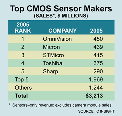
Toshiba holds a significant share of the market—and has supplied image sensors to 8 of the top 10 mobile phone manufacturers globally as ranked by Gartner Dataquest (Feb. 2006).
Toshiba employs over 300 engineers dedicated to the development and application engineering of imaging products. Two of the company’s dedicated wafer fabs, located in Iwate and Oita, Japan, are focused on CCD and CMOS image sensor manufacturing.
Toshiba is the only company that can claim leadership in both area image sensors (such as those found in camera phones) and linear image sensors (utilized in scanners).
Toshiba also put a nice market shares chart:
Toshiba image sensors deliver best-in-class image quality through continued innovations in:
1. Unique pixel structure development
2. Proprietary semiconductor process technology
3. Advanced micro lens and color filter technology
4. Proprietary image pipeline technology
Toshiba holds a significant share of the market—and has supplied image sensors to 8 of the top 10 mobile phone manufacturers globally as ranked by Gartner Dataquest (Feb. 2006).
Toshiba employs over 300 engineers dedicated to the development and application engineering of imaging products. Two of the company’s dedicated wafer fabs, located in Iwate and Oita, Japan, are focused on CCD and CMOS image sensor manufacturing.
Toshiba is the only company that can claim leadership in both area image sensors (such as those found in camera phones) and linear image sensors (utilized in scanners).
Toshiba also put a nice market shares chart:

Wednesday, November 22, 2006
Forum on Noise in Imagers on ISSCC 2007
The same prematurily published ISSCC 2007 advance program has interesting forum on imagers noise problems:
IMAGER DESIGN FORUM
F4: Noise in Imaging Systems
Organizer: Albert Theuwissen, DALSA, Eindhoven, Netherlands
Committee: Dan McGrath, Eastman Kodak, Rochester, NY
Jed Hurwitz, Gigle Semiconductor,
Edinburgh, United Kingdom
Hirofumi Sumi, Sony, Tokyo, Japan
Boyd Fowler, Fairchild Imaging, Milpitas, CA
Makoto Ikeda, University of Tokyo, Tokyo, Japan
Takao Kuroda, Matsushita, Kyoto, Japan
Johannes Solhusvik, Micron Technology, Pasadena, CA
Yonghee Lee, Samsung, Gyeonggi-Do, Korea
Noise in Imaging Systems has much in common with noise in the classical world of analog electronics, but imaging adds some very specific noise issues to consider. In many cases the electronic engineer only refers to temporal noise when discussing noise, but in an imaging system non-temporal noise sources also need to be taken into account. In addition, the perfect image sensor in a perfect camera still suffers from noise, because of the photon shot noise of the input signal.
This forum is organized to contribute to a better understanding of noise issues in imaging systems and to stimulate creativity in this field. The speakers at this forum are world experts in this area.
Takao Kuroda (Matsushita) will introduce the topic to begin the forum. The next talk, by Boyd Fowler (Fairchild Imaging), will discuss several noise mechanisms starting with the most important one, kT/C noise. The kT/C noise sets a fundamental detection limit on capacitive sensors. Therefore it is important to understand the factors that determine the kT/C noise and how this noise may be mitigated.
Bedrabata Pain (JPL) will speak on the topic of device-level noise. The pixels in imagers are becoming extremely small and several noise sources can be distinguished within every pixel. Shrinking the CMOS technology will put constraints on the pixel’s noise behavior.
A CMOS imager is usually a complex mixed analog-digital system-on-chip and circuit noise often dominates the total noise of the image sensor. The circuit noise is observed as a fixed pattern noise or a temporal random noise. The former is originated by device mismatches and is cancelled in the analog and/or digital domains, while the latter is more problematic. Shoji Kawahito (Shizuoka U) will discuss noise at the circuit level.
One level higher than the circuit is the system level. Each of the system elements plays an important role in determining the overall noise of the system. The optics may introduce noise in the form of stray signals, such as flare and ghost images, both of which result from internal reflections. A system-level view must also consider factors such as the pixel spectral response, which affects noise amplification, as well as the noise originating from power supply variation, timing jitter, and imperfect FPN cancellation circuits. The speaker invited to talk about system-level noise is Rick Baer (Micron Technology).
Random noise and distortion added to an image signal only matters when it can be seen. Seeing it however does not necessarily mean that it will be considered as a defect. Visual artists learn to use the features of a technology that impart a distinctive look to the resulting image for artistic goals. Jim Larimer (ImageMetrics) will review the properties of the human visual system that allow viewers to see distortion and noise in the temporal, spatial and intensity domains of the image, how the eye samples the signal and how this process can “beat” with capture and reconstruction methods.
The last presentation of the forum will highlight some algorithms used to cancel noise in images. Aleksandra Pizurica (Ghent U) will review some of the latest and best available multiresolution methods for noise reduction. Attention will be given to the following topics: estimation of the noise statistics from the input image (or video); construction of spatially adaptive denoising methods; motion estimation/compensation and noise suppression adapted to motion estimation reliability. In addition, some application specific topics, such as the use of “noise patterns” and camera reference frames for denoising digital camera images will be reviewed.
Although this forum focuses on imaging systems, the issues and techniques dealt with are also applicable to other emerging fields.
Micron 1.75um Pixel Performance on ISSCC 2007
Fukuoka Institute of Technology put out an advance ISSCC 2007 program, even though it's password protected on the official ISSCC site.
The program containts quite a few interesting papers. First is Micron's 1.75um imager presentation:
28.5 A 1/2.5 inch 8.1Mpixel CMOS Image Sensor for Digital Cameras
K-B. Cho, M. Lee, S. Eikedal, J. Solhusvik
Micron Technology, Pasadena, CA
A 1/2.5 inch 8.1Mpixel CMOS image sensor with 1.75μm pixel pitch is designed to operate at 2.8V for digital still camera applications and down to 2.4V in mobile applications. The chip uses top and bottom multiple channels with a double-data-rate analog signal readout at a rate of 96Mpixels/s, which results in total 192Mpixels/s. With the analog gain set to 15.875 and a 12b ADC the noise floor falls as low as 3.8e-, yielding a pixel DR of 63.8dB.
It's not clear what happened with 2e- noise floor that Micron announced about 1.5 year ago. Now the performance numbers are much more modest. Also, the small DR number shows the full well capacity is quite low, about 6Ke - too low to become a viable contender for digital camera market, or even for high end camera-phone market. After a 2-year work on 1.75um pixel development it looks like Micron hits a brickwall with pixel size shrink.
Another interesting presentation comes from Canon:
28.6 A 1/2.7 inch Low-Noise CMOS Image Sensor with Double CDS Architecture for Full HD Camcorders
H. Takahashi, T. Noda, T. Matsuda, T. Watanabe, M. Shinohara, T. Endo, S. Takimoto, R. Mishima, S. Nishimura, K. Sakurai, H. Yuzurihara, S. Inoue
Canon, Ayase, Japan
A 1/2.7 inch 1944×1092pixels CMOS image sensor with multi-gain column amplifier and double noise canceller is fabricated in a 0.18μm 1P3M CMOS process. It operates at 48MHz in a progressive scanning mode at 60fps. A 2T/pixel architecture and low optical stack with micro innerlens achieve 14.8ke-/lx·s sensitivity, 14ke- saturation, 3.7erms noise and 12.2e- dark current at 60°C.
The pixel size is about 3um here, quite outdated by now. However, the noise is quite good and dark current numbers are really astounding.
Another interesting paper came form Grass Valley and Thomson Silicon:
28.7 A 2/3 inch CMOS Image Sensor for HDTV Applications with Multiple High-DR Modes and Flexible Scanning
P. Centen(1), S. Lehr(2), V. Neiss(2), S. Roth(2), J. Rotte(1), H. Schemmann(2), M. Schrieber(2), P. Vogel(2), B-K. Teng(2), K. Damstra(1)
(1) Grass Valley, Breda, The Netherlands
(2) Thomson Silicon Components, Villingen, Germany
A 3T CMOS image sensor is designed with cost-effectiveness and a high degree of flexibility in mind. It supports an optimal interaction between imager and the external processing. An overall noise level of 11.5e- (4e- for the pixel alone) is obtained along with a Qmax of more than 15ke- per pixel. The design supports 1920(H)×1080(V)p90 and 1920(H)×1080(V)i180 at a data rate of 2.7Gb/s.
It's not clear how they achieved 4e noise for 3T pixel, combined with 15K full well. Quite an achievement for 3T design.
Other notable presentations are:
28.8 A MOS Image Sensor with Microlenses Built by Sub-Wavelength Patterning
K. Toshikiyo, T. Yogo, M. Ishii, K. Yamanaka, T. Matsuno, K. Onozawa, T. Yamaguchi
Matsushita Electric Industrial, Kyoto, Japan
A MOS image sensor has digital-microlenses implemented by sub-wavelength patterning of concentric SiO2 ring walls. The sensitivity at the periphery of the imager is 3000e-/lx·s. In comparison, the sensitivity at the periphery of a conventional imager is 1300e-/lx·s. Thus, extremely uniform brightness throughout the reproduced image is demonstrated even with an angle of incidence >45°.
28.4 A CMOS Image Sensor with a Column-Level Multiple-Ramp Single-Slope ADC
M. Snoeij(1), P. Donegan(2), A. Theuwissen(1,3), K. Makinwa(1), J. Huijsing(1)
(1) Delft University of Technology, Delft, The Netherlands
(2) DALSA, Waterloo, Canada
(3) DALSA Semiconductors, Eindhoven, The Netherlands
A CMOS image sensor uses a column-level ADC with a multiple-ramp single-slope (MRSS) architecture. This architecture has a 3.3× shorter conversion time than a classic single-slope architecture with equal power. Like the single-slope ADC, the MRSS ADC requires a single comparator per column, and, additionally, 8 switches and some digital circuitry. A prototype in a 0.25μm CMOS process has a frame rate 2.8× that of a singleslope ADC while dissipating 24% more power.
Tuesday, November 21, 2006
Flextronics Licenses HP Image Processing Technology
CNET: Flextronics has licensed digital imaging technology from HP and will begin to incorporate the technology into cell phones that hit the market in 2007. HP currently includes the same technology in its own digital cameras.
"There will be a number of cameras that will ship with this technology," said Joe Beyers, vice president of HP's IP licensing group. "This is core technology within the image capture process itself."
Flextronics makes phones for Motorola, Kyocera and Sony Ericsson, among others.
"There will be a number of cameras that will ship with this technology," said Joe Beyers, vice president of HP's IP licensing group. "This is core technology within the image capture process itself."
Flextronics makes phones for Motorola, Kyocera and Sony Ericsson, among others.
Sunday, November 19, 2006
Camera-Phone Image Quality Forum
Stanford University hosts Technical Forum on Camera Phone Image Quality on December 7, 2006.
Most known people from the Valley area presenting there. Here is the Forum's program:
Opening Remarks:
-- Joyce Farrell, Executive Director, Stanford Center for Image Systems Engineering
-- Lisa Walker, President, International Imaging Industry Association
Frontiers in Mobile Imaging
-- Video processing, encoding and transmission , Bernd Girod, Stanford
-- Advances and new applications for imaging sensors, Abbas El Gamal , Stanford
-- Perceptual quality metrics based on human vision, Brian Wandell, Stanford
Mobile Imaging (Lifestyle) Use cases and their impact on Quality
What's the Problem with Camera Phones?
Background of the CPIQ Initiative
Jim Peyton, Director of Standards and Technology, International Imaging Industry Association
Defining the CPIQ Eco-system
Gary Embler, Palm
Quantifying Camera Phone Image Quality
-- Resolution/speed : Don Williams, Eastman Kodak
-- Color /lighting: Paul Hubel, Foveon, and Jack Holm, Hewlett Packard
-- Image Quality Scaling: Bror Hultgren, Image Integration, Inc.
Evaluating Quality in Real World Applications:
Quality Evaluation in Dynamic Situations
How much Quality and at What price (Panel Session)
Concluding remarks
Friday, November 17, 2006
Eric Fossum's Digital Grain Paper
Eric Fossum published digital grain idea he presented on 2005 IEEE Workshop on CCDs and Advanced Image Sensors in Karuizawa, Japan and also at the Shizuoka University symposium on Nanoelectronics in Nov 2005 (link).
The patent on the digital grain idea belongs to Siimpel (based on Eric's info in DPReview forum).
Eric writes: The paper proposes using binary pixels (e.g. geiger-mode photodiodes) that I call jots and that are very very small. The jots are readout and OR'd together to create a grain, and the grains are then digitally developed by software to create pixels and an image. Grain size can be dynamically varied, both inter-frame and intra-frame.
Wednesday, November 15, 2006
Image Sensor Reverese Engineering in Electronic Design
John Parangalan from Chipworks wrote an interesting article in Electronic Design based on reverse engineering of Canon, Micron, Samsung and Sony sensors.
Tuesday, November 14, 2006
Banpil - Another Image Sensor Startup
I noticed them recently in EETimes article. Banpil's specialty is Multispectral Imaging Sensors.
CCD and CMOS image sensors technology are based on Si-technology, the detectable spectral ranges are limited to the wavelengths below 1 um where Si exhibits absorption. Besides, CCD and CMOS image sensors also have other shortcomings such as the inability to achieve high efficiency response combined with high quantum efficiency over a broad spectrum. It is highly desirable to design a monolithic sensor array, which could offer high bandwidth combined with high quantum efficiency over broad spectral ranges, and the possibility to rapidly and randomly address any pixel.
BANPIL has been issued with a patent on broadband image sensor capable of a broad spectral range and high sensitivity over a wide spectral range. This image sensor is capable of replacing today's CCD and CMOS sensors.
Monday, November 13, 2006
Hokkaido University Feedback Pixel
Hokkaido University team publishes yet another paper on feedback resetting of the pixel. This time the feedback reset is used to obtain picture smoothing. Here is the abstract of the paper:
CMOS Image Sensor Using Negative-Feedback Resetting to Obtain Variably Smoothed Images
Masayuki IKEBE and Keita SAITO
The authors are with the Graduate School of Information Science and Technology, Hokkaido University, Sapporo-shi, 060-0814 Japan.
We designed a CMOS image sensor capable of capturing variably smoothed images. This sensor uses a negative-feedback technique to set photodiode (PD) capacitance in the pixel circuit to any intermediate voltage during charge accumulation and it provides a neighboring-pixel operation by using their average value when resetting the PD capacitance. Smoothing-filter coefficients are changed by adjusting timing of the pixel-readout and neighboring-pixels operations. The performance of the proposed sensor was evaluated by SPICE simulation and numerical analysis.
Saturday, November 11, 2006
Siimpel Wraps Off Its New Product
After a long work in the stealth mode Siimpel presents a paper on the oncoming Electronic Imaging 2007 Conference:
MEMS digital camera, R. C. Gutierrez, T. K. Tang, R. J. Calvet, E. R. Fossum, Siimpel Corp. [6502-36]
I'm intrigued to see what came out of this.
Other notable papers are:
Mobile imaging (Invited Paper), K. Johnson, F. Xiao, J. Pincenti, Motorola, Inc. [6502-01]
Ultracompact optical zoom lens for mobile phone, K. Matsusaka, S. Ozawa, R. Yoshida, T. Yuasa, Y. Souma, Konica Minolta Opto, Inc. (Japan) [6502-02]
Camera-motion and mobile imaging, F. Xiao, J. Pincenti, G. John, K. Johnson, Motorola, Inc. [6502-03]
Autofocus survey: a comparison of algorithms, L. C. Shih, Cypress Semiconductor Corp. [6502-10]
Modeling of pixel reset associated wide dynamic range CMOS log image sensor, M. Hashimoto, Omron Automotive Electronics Technology (Germany); Y. Tani, Omron Corp. (Japan); J. Sochos, Omron Automotive Electronics Technology (Germany) [6502-04]
Leakage characteristics for the buried photodiode structure on CMOS image sensors, S. Lee, S. Lim, C. Lee, S. Bang, S. Kang, J. Park, J. Park, Dongbu Electronics Co., Ltd. (South Korea); R. A. Martin, S. Bae, Foveon, Inc. [6502-05]
CMOS color image sensors with silicon photodiode and overlaid organic photoconductive layer having narrow absorption band, S. Takada, M. Ihama, Fuji Photo Film Co.,Ltd. (Japan); T. Komatsu, T. Saito, Kanagawa Univ. (Japan) [6502-06]
Motion deblurring based on fusing differently exposed images, M. Tico, M. Vehvilainen, Nokia Research Ctr. (Finland) [6502-30]
Fast nonlocal means for image denoising, B. C. Radu, M. Vehvilainen, Nokia Research Ctr. (Finland) [6502-26]
CMOS image sensor noise reduction method for image signal processor in digital cameras and camera phones, Y. Yoo, S. Lee, W. Choe, C. Kim, SAMSUNG Advanced Institute of Technology (South Korea) [6502-27]
Friday, November 10, 2006
Super-Sensitive Gyro Sensor from Epson
Epson Toyocom announced super-sensitive gyro sensor XV-8000CB. The sensor is mainly intended for in-car GPS, but its sensitivity allows also a very efficient digital camera image stabilization.
Here is the sensor spec:
Here is the sensor spec:
| Item | Specification | Unit |
| Supply voltage | 4.75 to 5.25 | V |
| Operating temperature range | -40 to +85 | °C |
| Sensitivity | 25.0 | mV/deg/sec |
| Zero-point voltage | 2.5 | V |
| Zero-point voltage temperature variation | ±3.5 | % |
| Detection range | ±60 | deg/sec |
| Dimensions | 5.0 x 3.2 x 1.3 | mm |
Thursday, November 09, 2006
More about Mitsubishi Image Stabilization
A patent search reveals that the same guys from Mitsubishi filed a PCT patent application on image stabilized sensor. Most of the text is in Japanese, except of the abstract:
IMAGE PICKUP DEVICE
Abstract:
A first to an Nth (N is 2 or more) images are read (34) during a charge storing period of a charge storage means (31), the read first image is held by an image holding means (35), the held first image is shifted by 1/N of a moving quantity of an image pickup device by an image shifting means (36), and the shifted first image is added to the second image, and the image obtained by the addition is shifted again by 1/N and a third image is added. Such operations are repeated up to the Nth image (37). Camera shake correction can be performed without using a device having a special mechanism.
Sounds a bit similar to Sony's digital stabilization and Canon's one. Will see what's in the paper on ICCE.
Wednesday, November 08, 2006
Potentially Interesting Paper on ICCE 2007
The oncoming ICCE 2007 conference has an intriguing paper on image stabilization:
8.3-2 A NEW IMAGE-STABILIZING METHOD BY TRANSFERRING ELECTRIC CHARGES
Mitsuo Hashimoto, Tetsuya Kuno, Hiroaki Sugiura, Mitsubishi Electric Corp., Japan
As the name implies the image stabilization might be implemented inside an image sensor. This is certainly worth watching.
8.3-2 A NEW IMAGE-STABILIZING METHOD BY TRANSFERRING ELECTRIC CHARGES
Mitsuo Hashimoto, Tetsuya Kuno, Hiroaki Sugiura, Mitsubishi Electric Corp., Japan
As the name implies the image stabilization might be implemented inside an image sensor. This is certainly worth watching.
Sharp's new CCD with 1.88um Pixels
DPReview: Sharp announced 12MP 1/1.7" CCD with 1.88um pixels. Looks like almost the smallest pixel size CCD , other than Sanyo's 1.56um pixel FFT CCD announced almost a year ago.
Al-Manazir: New Camera-Phone Technical Blog
There is a new blog devoted to digital optics and camera-phones: Al-Manazir.
Among other basic things about camera-phone technology, it gives market shares chart. I'm not sure how credible is this data, as it has no reference to its source whatsoever. Here it is, anyway:
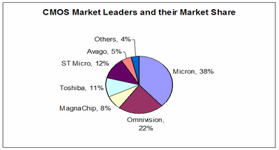
Among other basic things about camera-phone technology, it gives market shares chart. I'm not sure how credible is this data, as it has no reference to its source whatsoever. Here it is, anyway:

Saturday, November 04, 2006
IBM 0.18um CIS Process Data
Google cash reveals details of hidden IBM pdf file with CIMG7SF CIS process description.
First are IBM's sub-3um pixel parameters:
Dark Current: 100-300pA/cm @ 60C, which is equivalent to 34e/s @ 60C
Noise, Total: 30e rms @ 3Msps (including FPN)
Charge Capacity: 5630e/um, 10,300e
QE: 40% peak
Angle response:
10deg @ 70% of max, vertical
17deg @ 70% of max, horizontal
20deg @ 70% of max, diagonal
PRNU: 5% peak-to-peak, global
Image lag: 10e
Color closs-talk: 20% of Green, as measured in Red @ 650nm
Process: CIMG7SF
Wiring: Copper and aluminum
Process highlights:
Standard features:
■ Twin or triple-well CMOS technology on p- epitaxial p+ substrate
■ 4T/4S reference pixel
■ Photodiode defined with additional FEOL block masks
■ Thin Cu BEOL
■ Three and four levels of global metal
■ Fully integrated color filter array with webbed micro lenses
Optional features:
■ Vertical natural capacitor (VNCAP)
■ Nitride metal-insulator-metal (MIM) capacitor
■ Polysilicon RR resistor
■ Optional chip scale package
■ Electrically writable e-fuses
Process Description:
Lithography: 180 nm
Voltage (VDD): 1.8 V
Additional power supply options: 2.5 V / 3.3 V I/O
Standard NFET / PFET:
Lmin: 0.18 µm
Lp: 0.145 µm
Vt(Wdes/Ldes = 10 µm/0.18 µm): 0.40 V / -0.38 V
IDsat(Wdes/Ldes = 10 µm/0.18 µm): 610 µA/µm / 260 µA/µm
Ioff(Wdes/Ldes = 10 µm/0.18 µm): <25pa/um size="4">Thick-oxide NFET / PFET
Lmin: 0.4 µm
Lp: 0.29 µm
Vt: 0.56 V / -0.68 V
IDsat: 590 µA/µm / 225 µA/µm
Ioff: <2.5pa/um size="4">Available FET devices (maximum voltage):
Standard NFET/PFET (1.8 V)
Zero-Vt NFET (1.8 V)
Triple-well NFET (1.8 V)
Thick-oxide NFET/PFET (2.5 V)
Thick oxide zero Vt NFET (2.5 V)
Thick-oxide triple-well NFET (2.5 V)
Thick-oxide I/O NFET/PFET (3.3 V)
Thick-oxide triple-well NFET (3.3 V)
Here is the text portion of the document:
IBM Semiconductor solutions offers a leading-edge CMOS image sensor (CIMG) technology based on IBM’s industry-standard 180-nm CMOS technology family. Clients can choose appropriate devices and design tools to match their application requirements.
Base technology IBM CIMG7SF provides a highly competitive sub 3.0-µm, 4-transistor 4-shared (4T/4S) pixel architecture with an optimized transfer gate, which is ideal for mobile camera phone and digital still-camera applications. CIMG7SF also provides large reference pixels for high end digital still camera and emerging applications. The offering includes state-of-the-art micro lenses and color filters for exceptional quantum efficiency and angle response, along with pinned photodiode technology for reduced dark current. This technology uses aluminum wiring for the last metal level and copper wiring for the remaining metal levels. With thin back-end-of-line (BEOL) metal stacks and improved dielectric tolerance, CIMG7SF is ideal for multiple CMOS image-sensor applications.
The document is dated by July 2006.
Friday, November 03, 2006
SuperPix - One More CIS Startup
Yahoo-Finance: Tower Semiconductor announced another image sensor customer - SuperPix from China with 2MP sensor.
Initially, the products will be used in cellular phone and smart phone cameras to be retailed within the Chinese market, with projections to eventually expand sales internationally. The Chinese market is the fastest growing retail customer base for cellular products. The annual market for cellular and smart phone image sensors in China, alone, is projected to exceed 200M units in 2008 and 300M in 2010, with business volume of the image sensors projected to exceed $500M.
From SuperPix site:
Up to now, Superpix has successively developed a series of CIS-SOC chips including 1/3 inch UXGA, 1/4 inch SXGA and 1/6 inch VGA. The pixel size of these products spreads from 2.8um to 3.6um.
The company history is one of quite rapid product development:
2005, Apr: SuperPix Micro Technology (Beijing) Co., Ltd., setup on April,2005
2005, Sep: 1/6 inch VGA CIS-SOC developed successively
2005, Oct: 1/3 inch SXGA CIS-SOC developed successively
2005, Nov: 1/3 inch UXGA and 1/4 inch SXGA CIS-SOC developed successively
It's not immediately clear why this fast paced history log is ended a year ago. Company pages copyright notice reveals its connection with Micro Technology(Beijing)Co.,Ltd. If SuperPix is a spin-out of Micro, this can explain a very fast development schedule.
Thursday, November 02, 2006
Kodak Reports $100M of CIS Design Wins
Democrat & Chronicle: On the latest conference call Kodak's CEO Antonio Perez said Kodak believes that the sensor project could begin paying dividends soon. The company has been distributing its CMOS sensors for evaluation and has racked up $100 million of "design wins," in which a manufacturer chooses a particular product design over a competitor's.
The $100 million will not necessarily all translate into revenue, Perez said, "but I am trying to give you a sense of where we are ... we are building a portfolio of design wins with which I am very happy."
Theodore Franceschi, chief development officer and co-CEO at New Scale, said that in his discussions with handset manufacturers, he hasn't sensed a groundswell of demand for Kodak's sensor technology. But he quickly noted that the company does have a competitive strength in providing the imaging know-how for the sensors to produce better-quality images.
Analysts say that sales of camera phones are on their way to topping 1 billion a year by late 2008.
The scent of opportunity has also attracted a small Victor startup company with pioneering technology in providing miniaturized motors that can power zoom lenses or auto focus functions in camera phones. That's New Scale Technologies, which is working with Tamron Co. Ltd., a leading maker of precision optics based in Japan. Tamron is licensing New Scale's technology for use in Tamron's optical imaging assemblies, which include digital still cameras, camcorders and mobile phone cameras.
Dongbu and Siliconfile Trumpet 0.13um Era
Yahoo-Finance: Dongbu and Siliconfile announced jointly developed 0.13um process generation. Volume production of CIS devices using the new process is expected to begin during the first quarter of 2007.
The most strange thing about this press-release is that there is no mention of pixel size - one of the best metrics of process advances.
The new process uses a 3-layer aluminum interconnect. Distance between the photodiode and the micro lens has been reduced to less than 4 microns. Here the press release states "This compares to a 5-micron distance in CIS chips from the world's largest CIS device manufacturer, Micron Technology Inc." This is quite a rare direct comparison statement for an official press-release. Also, the data about Micron seems to be a little outdated.
The claim also improvements in color quality in terms of resolution, gray scale, relative illumination and color crosstalk among red-green-blue pixels, thereby improving sensitivity by more than 20 Percent.
Af for the next step, Dongbu is targeting early 2008 to qualify a CIS process at the 110nm node for volume production.
Wednesday, November 01, 2006
TrueImaging Start-Up Company
Another image sensor startup just came to my attention: TrueImaging Technology (San Jose, CA). It offers "unique "analog-free" ultra high dynamic range CMOS Image Sensors for cell phone cameras and multi-megapixel digital cameras". Its "patented technology enables superior image quality with better edge precision in sunlight conditions and vastly improved clarity in low-light conditions. TruImaging raises the bar above all the other analog-based image sensor players by bridging the quality/cost gap -- providing high CCD quality at low CMOS cost and low CMOS power consumption."
Here is what TrueImaging site says about its technology:
Here is what TrueImaging site says about its technology:
TruImaging's patented oversampling technology is critically strategic to cell phone camera OEMs and ODMs -- because it directly overcomes the "limitation of electrons" when cell camera pixel size needs to scale from 4um down to 3um and below. This is a physical limitation for all the analog-based conventional Active Pixel Sensors (APS) and CMOS approaches scaling to multi-megapixel cell cameras (1, 2, 3MP).
As focal plane resolution increases and lower frame rate (with longer integration time) is required for low light conditions with reduced photo diode sensitivity, output data rate is a serious problem for all analog readout players where noise bandwidth increases proportionally to the amount of data being transmitted. TruImaging addresses the noise sources by being digital at the pixel level with oversampling. TruImaging overcomes the "limitation of electrons" by effectively increasing well capacity, which increases signal and signal-to-noise ratio, which reduces the effects of shot noise and KTC noise -- beyond all other approaches. More light capability means better image quality.
TruImaging Technology provides unsurpassed ultra high dynamic range and significantly increased sensitivity necessary for low light level performance. This translates into "Day/Night Vision", "Indoor/Outdoor", "In the sun/out of the sun", flashless cell phone cameras... affordably.
- Integrated digital conversion on focal plane for digital cameras.
- Analog to digital conversion is at each pixel. Thereby, eliminates all analog electronics for improved reliability and reduced cost. No precision analog or trim to fit components are used.
- 100% pure digital circuitry implementation of analog to digital function with no analog ADC circuitry.
- Proven to be extremely low power compared to all other focal plane design methods.
- Exceeds the capabilities of analog and other digital approaches in linearity, dynamic range and signal to noise ratio.
- Uses generic CMOS logic manufacturing process.
- SoC integration friendly.
Subscribe to:
Posts (Atom)